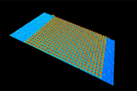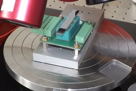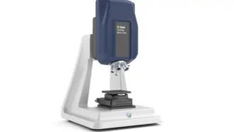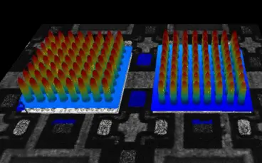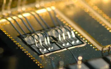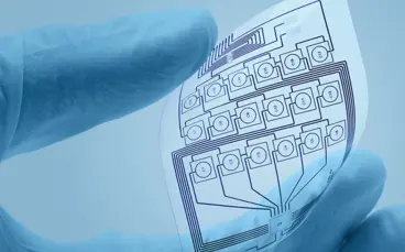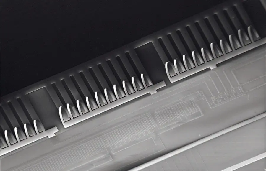
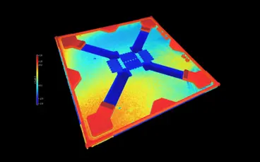
微结构MEMS芯片表面细节高分辨扫描显示,凸显纳米级精密光学测量技术应用。

 微结构和微技术计量学

微结构测量与微技术测试

在消费电子、汽车、可穿戴设备以及医疗科技等领域,功能组件的小型化催生了大量的应用与创新。微机电系统(MEMS)和微光学技术对精密测试有着极高的要求,给相应的测量技术和测试工具带来了新的挑战。复杂的微结构需要进行全面的分析,最为理想的是开展高分辨率( μm ~ nm 级别)的面扫描检测,从而深入了解其质量与功能方面的特性。

Polytec 的光学测量解决方案,不仅能够对表面的形貌、形状以及结构细节进行表征,还可以对微机电系统和微系统的动态运动情况以及性能表现进行测试 。

微结构静态形貌测量

微结构及微机电系统 MEMS,需严格契合公差标准,才能保障功能稳定与使用期限,同时要避免微观结构遭受物理损伤。因此,非接触式光学表面特性分析,是无损检测微技术、评估表面形状与粗糙度等参数的关键。Polytec 光学计量解决方案,可对微结构和微系统开展无干扰、可重复测量。​

TopMap 3D 表面测量基于相干扫描干涉技术,能扫描高度数据,数秒内采集数百万个表面测量数据,不受材料限制,无论是数控加工后的粗糙材质,还是晶圆类光滑反光材料,都能精准测量。其智能表面扫描技术,可轻松测量样本的不同反射区域。​

微结构静态形貌测量广泛应用于微传感器、微执行器检测,金属纹理板、密封表面或机加工表面研究 —— 这些场景都需确保良好润滑。此外,在化妆品、医疗技术领域的生物医学样本研发中,该技术也发挥着重要作用。
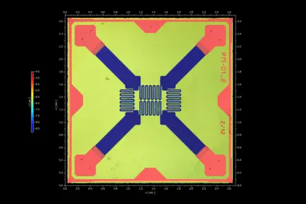
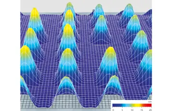
Colored 2D areal surface profile of a MEMS pressure sensor showing detailed microstructure and topography with scale bars.
Areal surface profile of MEMS pressure sensor (courtesy: CIS) as 2D/3D profile. Courtesy:CiS Forschungsinstitut für Mikrosensorik GmbH
Microscopic topography of MEMS microstructure showing detailed form and height profiles for precise optical metrology analysis.
Analyze MEMS and microsystems form, topography and capture height data on an entire area
Detailed view of a Lab-on-a-Chip device assessing microchannel depth, parallelism, and surface roughness for fluid transport.
Assesment of biomedical probes like LOC (Lab-on-a-Chip) devices, evaluating channel depth, parallelism or defined micro roughness for fluid transportation
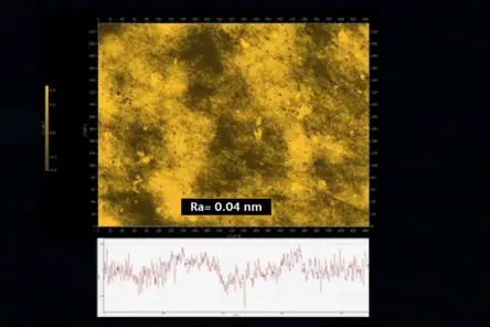
High-resolution surface roughness measurement of polished silicon showing Ra 0.04 nm with detailed microscopic texture and profile graph.
High-resolution roughness measurement <1nm; sample data of a polished silicon surface
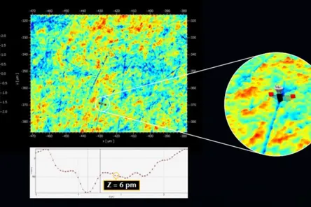
Sub-nanometer surface topography map with color-coded roughness data and cross-section graph measuring 6 pm height variation.
Characterizing small details and microstructures with sub-nanometer resolution; sample data of an optical polished surface
Microscopic color-coded surface roughness map with cross-sectional profile of a polished wafer, highlighting microstructure topography.
Micro roughness with cross section of a wafer surface
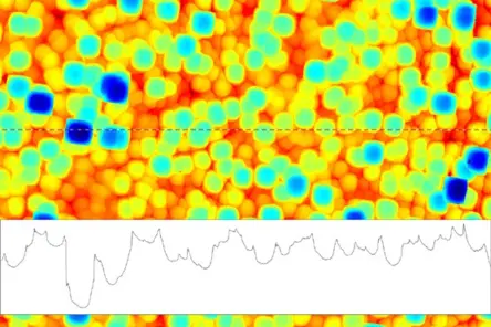
3D topography map showing nanometer-resolution surface height data of a microstructured array with color-coded elevations.
Analyze microstructure topography with nanometer resolution

Downloads

联系Polytec专家

测量您的微机电系统(MEMS)和微结构,并与您一同展开分析

MEMS 动态测量

主动式微机电元件(如 MEMS 执行器和传感器)仅靠电气表征不够,需先进光学测量技术。Polytec的MSA 显微式激光测振仪,可全面表征微系统动态特性。该 MEMS 测试系统能精准评估高分辨率表面形貌和元件动态特性。

测量技术

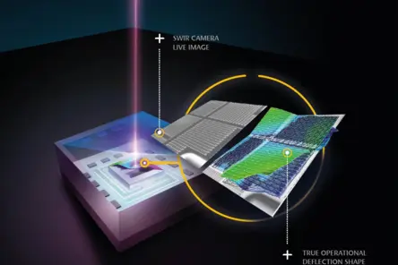
其动态特性测量运用激光多普勒测振技术,可进行 GHz 宽带测量,高分辨率呈现元件模态振型和真实相位,常用于模型验证。专利 IRIS 技术可透过硅封装检测 MEMS 动态,实现成品测试。
动态微机电系统表征

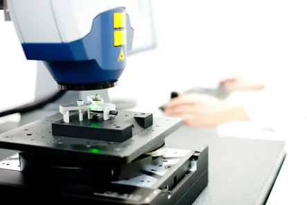
High-precision non-contact optical metrology system analyzing microstructures on a compact mechanical probe for MEMS testing.
Non-contact analysis of tiny mechanical and biological probes in 3D
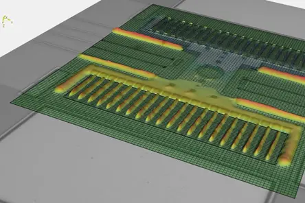
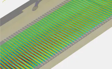
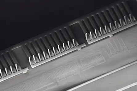
Optical full-field vibration analysis at 6.8 kHz of a MEMS comb drive showing displacement and modal behavior.
Full-field, optical vibration analysis of a combdrive at 6.8 kHz
IR laser beam analyzing MEMS device through silicon cap, showing SWIR camera live image and deflection shape measurement.
Micro System Analyzer IRIS using IR laser for measuring MEMS through Si caps in final state
High-precision vibration measurement system testing Si capped MEMS for modal analysis in microtechnology research.
Vibration measurement as a service for modal testing inside Si capped MEMS
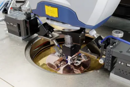
MSA-650 IRIS microscope setup for precise optical measurement and analysis of Si capped MEMS microstructures and microsystems.
MSA-650 IRIS patented measurement technology for analysis on Si capped MEMS
MEMS cantilever vibration analyzed in time and frequency domain using Polytec optical measurement software.
MEMS cantilever resolved in time and frequency domain with optical vibration measurement from Polytec

微结构的接触式与光学测量方法对比

接触式表面测量技术在微结构分析上存在局限性。借助二维轮廓线,难以获取整个表面的复杂结构细节,且测量耗时久。这类测量常以粗糙度轮廓线为参考,开展后续评估。此外,触针测量会在表面留痕、造成自身磨损,影响测量重复性。

非接触式光学检测技术,在机械工程精密表面检测中优势突出。它测量可重复,不会产生废品,在全表面测量和 100% 抽检场景下,效率更高、成本更低。

我们可为您测量样品,并通过免费可行性研究,展示实际成效!
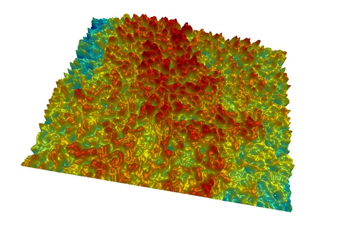
3D topography map of a microstructured surface showing detailed surface roughness and texture in red, yellow, green, and blue.

相关产品

Micro.View

Micro.View是一款紧凑型台式光学轮廓仪,操作简便。作为高性价比的检测工具,它可对精密加工表面进行亚纳米级分辨率的检测,适用于粗糙度、微观结构及其他表面细节的评估。
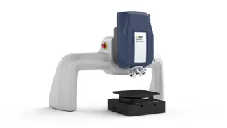
Micro.View+

Micro.View+ 是一款基于显微镜平台的高端表面轮廓仪,支持自动化操作与彩色成像。其能够实现与操作人员无关的、高重复性的粗糙度与纹理分析,可同时满足实验室研发与生产现场的质量控制需求。
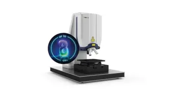
MSA-600显微式激光测振仪

MSA-600显微式激光测振仪专为MEMS与微结构测量打造,集成三维静态与动态特性测试能力,是一款一体化光学测量解决方案。其在加速产品研发流程、强化质量管控方面表现出色,并可集成至商用探针台用于晶圆级测试。目前测量频率已扩展至8 GHz。
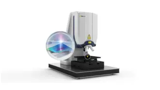
MSA-650 IRIS显微式激光测振仪

这款创新且已获专利的MSA-650 IRIS显微式激光测振仪具备红外(IR)功能,可通过硅封装对面内和面外运动进行表征,无需接触即可测量高达25 MHz的真实MEMS动态特性,且无需对器件进行预处理或去封装。
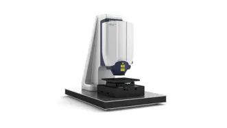
MSA-100-3D显微式激光测振仪

3D显微式激光测振仪可同时记录三个空间方向上的振动分量。其光学测量系统能够对平面内和平面外的振动分量进行高分辨率的三维振动分析,频率范围从直流到25 MHz,振幅分辨率可达亚皮米量级。
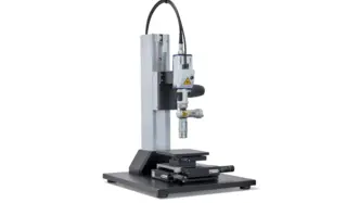
MSA-060显微式激光测振仪

使用MSA-060显微式激光测振仪,踏入微系统振动分析领域。该设备能够以激光级精度,对小型组件和微系统的振动及动力学特性进行全表面范围的记录和可视化,测量频率范围从直流(DC)到24 MHz。微系统分析仪利用测量激光,以完全非接触、非侵入的方式揭示小型组件的真实动力学特性。
Smiling man in casual dark sweater stands confidently in modern office environment with blurred background.

与Polytec专家进行交流

Our experts are ready to support your projects with tailored measurement solutions or support you in measuring what matters — get in touch with us today.

下載

請填寫表格,您將在幾分鐘內透過電子郵件收到下載連結。