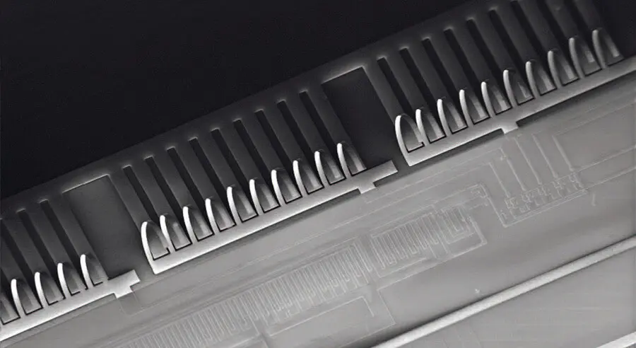
Measuring microstructures, testing microtechnology
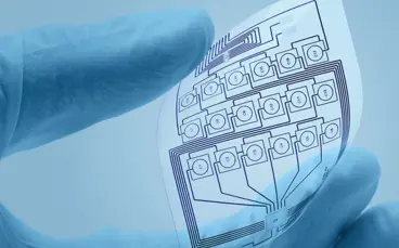
Miniaturizing functional components enables numerous applications and innovations, whether in consumer electronics, automotive, wearables or medical technology. Micro-electromechanical systems (MEMS) or microoptics place high demands regarding sophisticated testing, presenting new challenges to respective measurement technology and testing tools. Complex microstructures require a comprehensive analysis, ideally including areal inspection with high resolution (µm to nm range), revealing insights regarding quality and functionality.
Polytec optical measurement solutions allow characterizing both the areal topography, form and structural details as well as testing the dynamic motion and behaviour of MEMS and microsystems.
Static topography measurement of microstructures
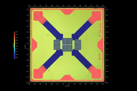
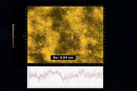
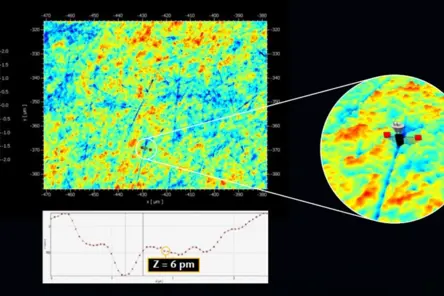
Microstructures and MEMS as micro-electromechanical systems must comply with tight tolerances in order to guarantee functionality and the life-time. Physical influences on the microscopic structures should be avoided. Therefore, optical non-contact surface characterization is key to inspecting microtechnology in a non-destructive and non-invasive way, evaluating surface parameters like form and roughness. Polytec optical metrology solutions provide non-reactive and reproducible measurements on microstructures and microsystems.
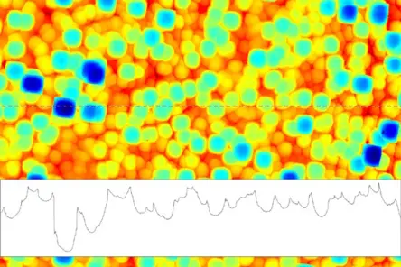
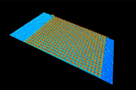
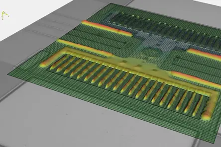
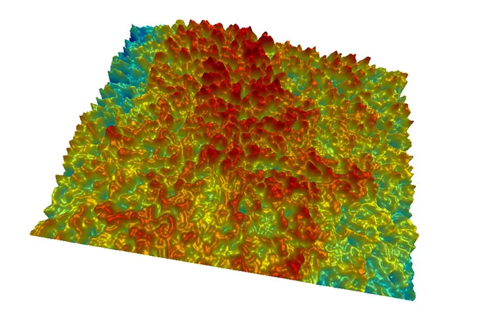
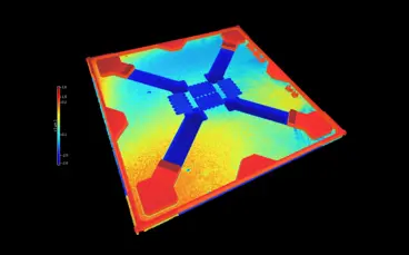
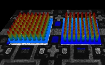
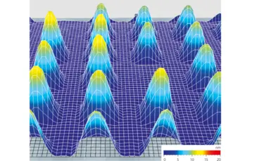
TopMap 3D surface metrology characterizes microstructures based on coherence scanning interferometry, scanning height data and collecting millions of measurement data on an entire surface within a few seconds regardless of the materials - whether matt or rough texture after CNC machine processing or smooth and reflective like wafers. Smart surface scanning technology facilitates measurements on varying reflective areas of a test specimen. Typical static topography measurements of microstructures are used on microsensors and actuators, investigations on structured metal sheets, sealing surfaces or machined surfaces, where proper lubrication must be secured, or research and development of biomedical samples for cosmetics and medical technology.
Downloads
Get in touch with our experts
Get in touch with our experts
We measure your MEMS and microstructures and analyze them with you!
Measuring MEMS dynamics
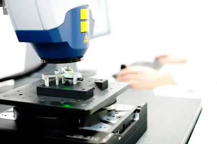
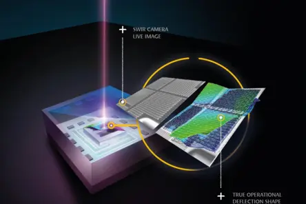
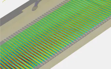
Active micro-electromechanical components such as MEMS actuators and MEMS sensors demand sophisticated optical measurement technology, since electrical characterization alone is not sufficient. The line of MSA Micro System Analyzers from Polytec is designed for the thourough characterization of the dynamic behaviour of microsystems. These MEMS testing systems enable the precisely assesment of both the high-resolution surface topography and the dynamic component like motion. The dynamic measurement uses laser Doppler vibrometry, allowing for broadband measurements up to the GHz range, visualizing mode shapes of components with a high amplitude resolution and true phase, often used for model validation. The patented IRIS technology even captures MEMS dynamics through intact Si encapsulation, enabling to test MEMS in final state. Find out more here!

Tactile vs optical measurement of microstructures
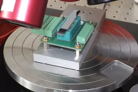
Tactile surface measurement technologies face limits when it comes to microstructure analysis since the complex structural details are difficult to be transferred over an entire surface using a 2D profile line or it can become quite time-consuming. A reference line is used here, often referred to as roughness profile, often becoming the basis for further evaluation. Tactile measurements with stylus tips can leave marks on the surface and are subject to wear, which can affect repeatability over time. A non-invasive optical testing method shows particular advantages for precision surfaces in mechanical engineering, offers reproducible measurements, does not lead to NOK parts and proves to be faster and more cost-effective for full-areal measurements or 100% inspections in production or research.
We measure your samples and show what's possible in free feasibility studies!
Related products
Micro.View
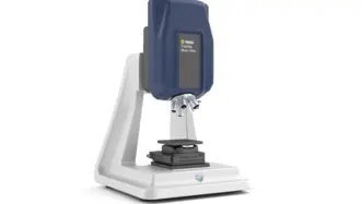
TopMap Micro.View® is an easy to use optical profiler in a compact table-top setup. Choose Micro.View® as the cost-effective inspection tool for examining precision-engineered surfaces down to the sub-nm range, for inspecting roughness, microstructures and more surface details.
Micro.View+
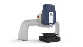
Advanced microscope-based surface profiler with automation and color imaging. Micro.View+ enables repeatable, operator-independent roughness and texture analysis—ready for lab and production use.
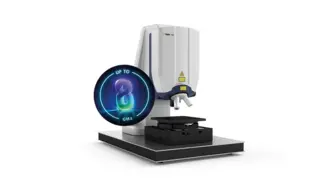
MSA-600 Micro System Analyzer
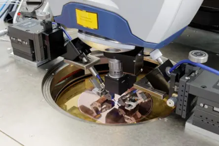
The all-in-one optical measurement solution for static and dynamic 3D characterization of MEMS and microstructures- now for up to 8 GHz! The MSA-600 enhances microsystem development and quality inspections - also allowing testing on wafer-level when integrated into commercially available probe stations.
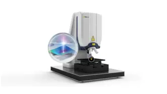
MSA-650 IRIS Micro System Analyzer
The innovative and patented MSA-650 IRIS Micro System Analyzer with IR capability allows for measuring true MEMS dynamics up to 25 MHz by characterizing both in-plane and out-of-plane motions through silicon encapsulation without contact, without need for preparing nor decapping the device.
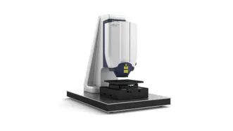
MSA-100-3D Micro System Analyzer
The 3D Micro System Analyzer records vibration components in all three spatial directions at once. The optical measurement system enables high-resolution 3D vibration analysis from DC up to 25 MHz with amplitude resolutions in the sub-picometer range, for both in-plane and out-of-plane vibration components.
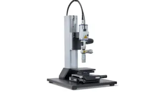
MSA-060 Micro System Analyzer
Use the MSA-060 for entering the world of microsystem analysis. Record and visualize vibrations and dynamics of small components and microsystems with laser precision over an entire surface from DC to 24 MHz. Micro System Analyzers use measurement lasers, revealing the true dynamics of small components in a completely non-contact and non-invasive way.


Talk to our experts
Our experts are ready to support your projects with tailored measurement solutions or support you in measuring what matters — get in touch with us today.