MEMS微細構造の光学式非接触測定による高精度な表面トポグラフィと形状評価

マイクロテクノロジー分野における計測学

微細構造物やマイクロテクノロジー分野における光学式測定

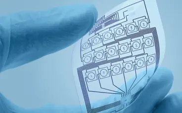
機能部品の小型化により、民生用電子機器、自動車、ウェアラブル機器、医療技術など、さまざまな分野で数多くのアプリケーションやイノベーションが生まれています。微小電気機械システム (MEMS) やマイクロオプティクスでは、高度なテストに対する要求が増え、それぞれの測定技術やテストツールに新たな課題が生まれています。これらの複雑な微細構造においても、品質と機能に関するさらなる分析や評価のために包括的な測定が必要であり、高解像度 (µm から nm の範囲) の面測定も行われています。

ポリテックの光学式測定ソリューションは表面トポグラフィ、形状、詳細構造だけでなく、MEMS およびマイクロシステムの動特性や動作測定、評価することができます。

微小構造物に対する静的測定:トポグラフィ測定

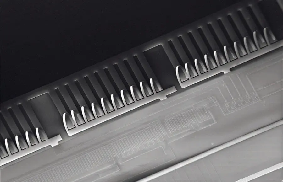
微小構造物と MEMS (微小電気機械システム)は、機能性と寿命を保証するための厳しい要求仕様に準拠する必要があります。その評価にあたって、微細構造への物理的影響は避けなければなりません。したがって、非接触である光学表面特性評価は、非破壊的かつ非侵襲的な方法として、マイクロテクノロジーを検査し、形状や粗さなどの表面パラメータを評価するための鍵となります。ポリテックの光学式測定ソリューションは、微小構造物とMEMSを含めたマイクロテクノロジーデバイスに対して物理的影響を抑え、再現性の高い測定を提供します。

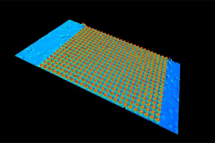
TopMap 3次元表面形状測定システムは 垂直走査低コヒーレンス干渉法により、CNC旋盤後のマット表面や粗いテクスチャ、ウェーハのように滑らかで鏡面状のテクスチャ、といった違いに依らず短時間で数百万点の高さデータを収集することで微細構造を特徴を捉えます。ポリテックのスマートスキャンテクノロジーは、反射度合に違いがあるテストサンプルであっても測定を容易にします。微細構造における一般的な静的トポグラフィ測定は、マイクロセンサやアクチュエータ、適切な潤滑を確保する必要がある構造化金属シート、シーリング表面、または機械加工表面の調査といった工業用途だけでなく、化粧品や医療技術用の生物医学サンプルの研究開発にも使用されています。nology.
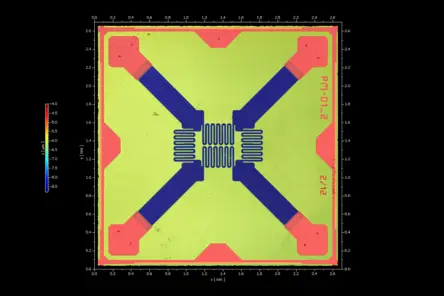
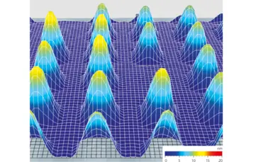
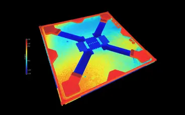
Colored 2D areal surface profile of a MEMS pressure sensor showing detailed microstructure and topography with scale bars.
Areal surface profile of MEMS pressure sensor (courtesy: CIS) as 2D/3D profile. Courtesy:CiS Forschungsinstitut für Mikrosensorik GmbH
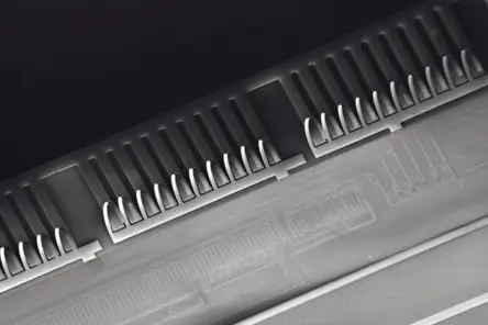
Microscopic topography of MEMS microstructure showing detailed form and height profiles for precise optical metrology analysis.
Analyze MEMS and microsystems form, topography and capture height data on an entire area
Detailed view of a Lab-on-a-Chip device assessing microchannel depth, parallelism, and surface roughness for fluid transport.
Assesment of biomedical probes like LOC (Lab-on-a-Chip) devices, evaluating channel depth, parallelism or defined micro roughness for fluid transportation
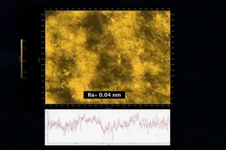
High-resolution surface roughness measurement of polished silicon showing Ra 0.04 nm with detailed microscopic texture and profile graph.
High-resolution roughness measurement <1nm; sample data of a polished silicon surface
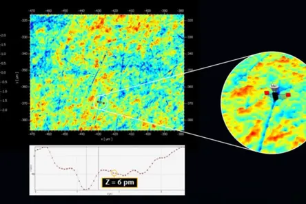
Sub-nanometer surface topography map with color-coded roughness data and cross-section graph measuring 6 pm height variation.
Characterizing small details and microstructures with sub-nanometer resolution; sample data of an optical polished surface
Microscopic color-coded surface roughness map with cross-sectional profile of a polished wafer, highlighting microstructure topography.
Micro roughness with cross section of a wafer surface
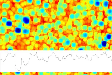
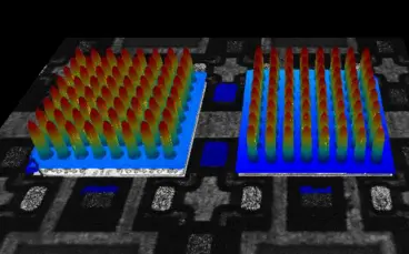
3D topography map showing nanometer-resolution surface height data of a microstructured array with color-coded elevations.
Analyze microstructure topography with nanometer resolution

Downloads

担当者へ問い合わせ

実機デモや計測サービス、レンタルサービスもポリテックなら対応可能

MEMSの動特性評価

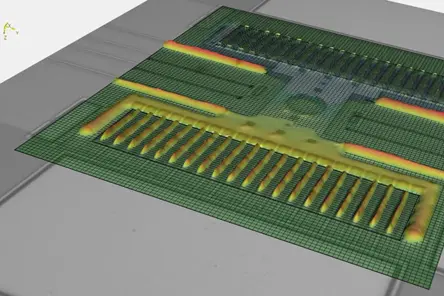
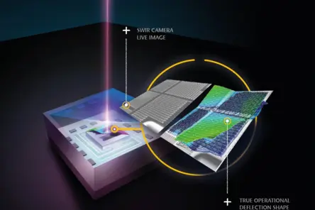
MEMSアクチュエータや MEMSセンサなど可動部のある微小電気機械コンポーネントは、電気特性評価だけでは不十分であり、その動特性を把握するためには高度な光学式測定技術が必要です。ポリテックのMSA マイクロシステムアナライザシリーズは、マイクロシステムの動特性や動作を評価することを目的に設計されています。このMEMSテストシステムでは、高解像度の表面トポグラフィと動的コンポーネントの動きの両方を正確に評価できます。動的測定ではレーザドップラ振動測定法を使用し、GHz 範囲までの広帯域測定が可能で、コンポーネントのモード形状を高い振幅分解能と位相情報から視覚化します。これはCAEモデルを検証する際の比較データとしてよく使用されます。また、特許取得済みの IRIS技術を採用した機種では、 Siキャップで封止された MEMS の動特性をキャップ越しに測定できるため、パッケージ化したMEMSの動特性評価が可能です。

詳細は以下でご覧いただけます。 
MEMSの動特性評価

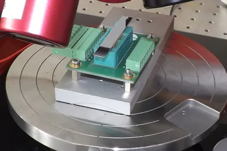
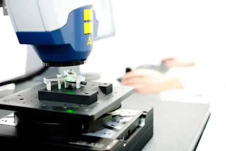
High-precision non-contact optical metrology system analyzing microstructures on a compact mechanical probe for MEMS testing.
Non-contact analysis of tiny mechanical and biological probes in 3D
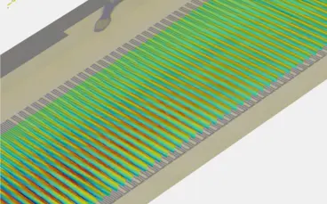
Optical full-field vibration analysis at 6.8 kHz of a MEMS comb drive showing displacement and modal behavior.
Full-field, optical vibration analysis of a combdrive at 6.8 kHz
IR laser beam analyzing MEMS device through silicon cap, showing SWIR camera live image and deflection shape measurement.
Micro System Analyzer IRIS using IR laser for measuring MEMS through Si caps in final state
High-precision vibration measurement system testing Si capped MEMS for modal analysis in microtechnology research.
Vibration measurement as a service for modal testing inside Si capped MEMS
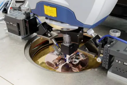
MSA-650 IRIS microscope setup for precise optical measurement and analysis of Si capped MEMS microstructures and microsystems.
MSA-650 IRIS patented measurement technology for analysis on Si capped MEMS
MEMS cantilever vibration analyzed in time and frequency domain using Polytec optical measurement software.
MEMS cantilever resolved in time and frequency domain with optical vibration measurement from Polytec

表面形状測定における接触式 vs 光学式

微細構造の分析において、接触式表面測定技術には限界があります。複雑な構造物を 2Dプロファイルラインを使用して表面全体の詳細を得ることがそもそも困難であったり、可能であったとしても非常に時間がかかります。また、粗さプロファイルと呼ばれる曲線を用いてさらなる評価を行うことがよくありますが、スタイラスチップを使用した接触式測定では、被測定物の表面に傷がついたり、チップ自体が摩耗することで時間の経過とともに再現性に影響を与える可能性があります。非接触の光学式表面測定技術は、機械工学における精密表面に特に有利であり、常に再現性の高い測定が可能です。そのため研究開発における表面全体の測定や、不良品を取り除くための生産ラインにおける100% 検査などにおいて、より高速でコスト効率が高いことがメリットとして挙げられます。

実際の測定対象物を用いたデモ測定もご相談可能です。ぜひお問い合わせください。
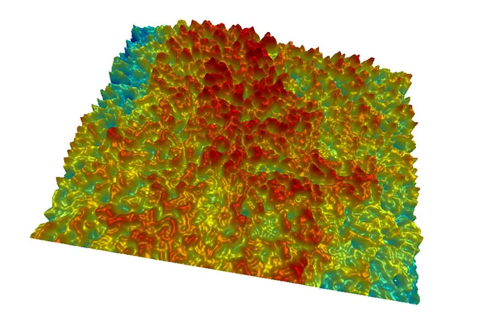
3D topography map of a microstructured surface showing detailed surface roughness and texture in red, yellow, green, and blue.

関連製品

Micro.View

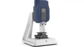
TopMap Micro.View® is an easy to use optical profiler in a compact table-top setup. Choose Micro.View® as the cost-effective inspection tool for examining precision-engineered surfaces down to the sub-nm range, for inspecting roughness, microstructures and more surface details.
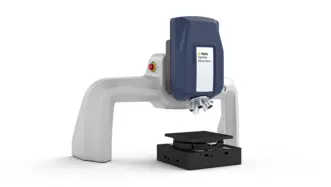
Micro.View+

Advanced microscope-based surface profiler with automation and color imaging. Micro.View+ enables repeatable, operator-independent roughness and texture analysis—ready for lab and production use.
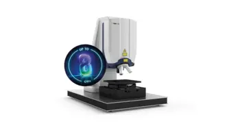
マイクロシステムアナライザ MSA-600

MSA-600 は、MEMS や微細構造の静的・動的な 3D 特性を測定するオールインワン光学測定ソリュー ションで、最大 8GHz まで対応します。MSA-600は、マイクロシステム開発および品質検査を強化し、市販のプローブステーションに組み込むことにより、ウェーハレベルでのテストも可能にします。
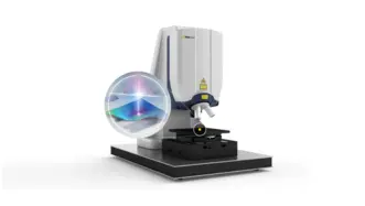
マイクロシステムアナライザ MSA-650 IRIS

MSA-650 IRIS マイクロシステムアナライザ は、赤外線レーザを採用した特許取得済みの革新的な顕微鏡型レーザドップラ振動計で、測定周波数帯域は最大25 MHzで、シリコンキャップ越しにマイクロシステムを測定することができ、デバイスに接触したりデキャップすることなく、真のMEMSダイナミクスを明らかにします。
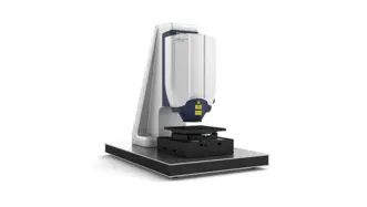
マイクロシステムアナライザ MSA-100-3D

MSA-100-3Dは、3次元におけるXYZ3軸振動成分を一度に測定します。非接触光学測定でありながら、面内および面外振動成分の両方において、DCから最大25MHzまでの高分解能3D振動解析をサブピコメートルレベルの振幅分解能で実現します。
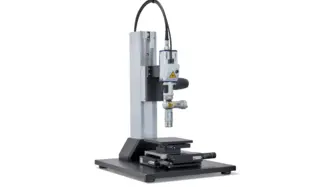
マイクロシステムアナライザ MSA-060

顕微鏡型レーザドップラ振動計のエントリモデルです。他のモデルはレーザが測定物表面をスキャンするのに対し、MSA-060は電動ステージによる多点計測で、DCから24 MHzの小さな部品の表面全体の振動を非接触で測定、可視化することができます。
Smiling man in casual dark sweater stands confidently in modern office environment with blurred background.

担当者へ相談

Our experts are ready to support your projects with tailored measurement solutions or support you in measuring what matters — get in touch with us today.

ダウンロード

フォームにご記入ください。数分以内にダウンロードリンクをメールでお送りします。