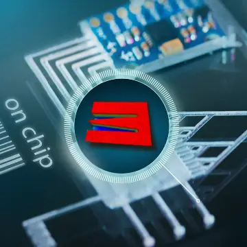
Securing functionality of lab-on-a-chip devices
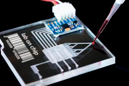
Microfluidic lab-on-a-chip systems, short for LoC, implement a multitude of occurring processes on the smallest of spaces. Lab-on-a-chip enable the analysis of liquids on a compact chip for process analytics and online diagnostics of biological, chemical or physical processes. Lab-on-a-chip devices use the capillary force for transporting very small quantities of a fluid in the range of a few picoliters (pL) or microliters (mL).
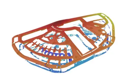
With non-contact measurement technology such as the TopMap 3D surface metrology, you can inspect the dimensional accuracy of the microfluidic channel of a lab-on-chip, evaluate the LoC channel depth or channel width with high precision, determine the volume or measure flatness over the entire surface of the lab-on-a-chip device.
Quality & process control of lab-on-a-chip production
The research and development service expert Hahn-Schickard develops intelligent products with microsystems technology from the idea to manufacturing. Together with industrial partners, Hahn-Schickard realizes innovative products and technologies in the fields of sensor technology, intelligent embedded systems for the Internet of Things (IoT), artificial intelligence (AI), lab-on-a-chip (LoC) and analytics as well as electrochemical energy systems.
In their lab-on-a-chip design for turberculosis tests, one of the challenges in the lab-on-a-chip production process is to precisely match the height of the sealing tools to the cartridge. If the height is too low, the sealing force is too low and the cartridges are not tight. If the height is too high, pressure splashes occur and melt can block the fine channels.
Choose the right surface profiler with confidence—let us run a feasibility study with your sample.


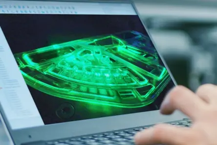
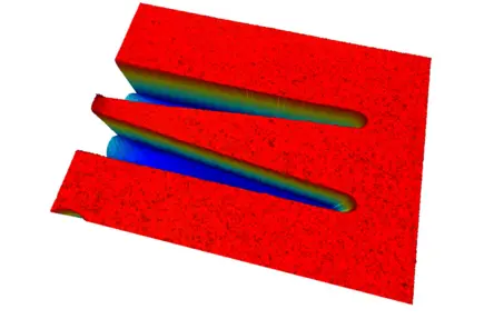
Applying the sealing film to the cartridges of our lab-on-a-chip is challenging: first, there is the demand of achieving a high seal strength without closing the fine channels of the cartridge during bonding. Secondly, production tolerances regarding the injection molding thicknesses cannot be eliminated completely, which has to be compensated when sealing. To adjust the sealing tool precisely, we measure the height levels of the cartridge using a scanning whitelight interferometer. This 3D measurement data then forms the basis for designing the sealing tool.
Lab-on-a-chip crucial parameters step-height, channel depth & flatness
With a large field-of-view (FoV) and high vertical resolution, the TopMap optical profilers allow a straightforward examination of lab-on-a-chip channel depths and geometrical inspection of the entire lab-on-chip by a single measurement, that creates millions of data points within just seconds. The telecentric optical design of the white-light interferometers shows a parallel light beam path, enabling to capture the channel bottom of lab-on-a-chip devices without shadowing effects that cause blind spots on the measurement data. The microscope-based profilersof the TopMap series focuson inspecting microsystems or structural details, roughenss evalatuation and more. Keeping the z-axis resolution constant, TopMap optical profilers allow a quick and easy adaption of the lateral resolution to changing measuring tasks by simply changing lenses.
Suitabel 3D surface profiler
Micro Profiler
Micro.View profiler systems are optimized for measurements with sub-nanometer resolution. With focused optics and high vertical resolution they enable detailed analysis of microstructures, surface finish and material distribution where even the smallest deviations matter.
Macro Profiler
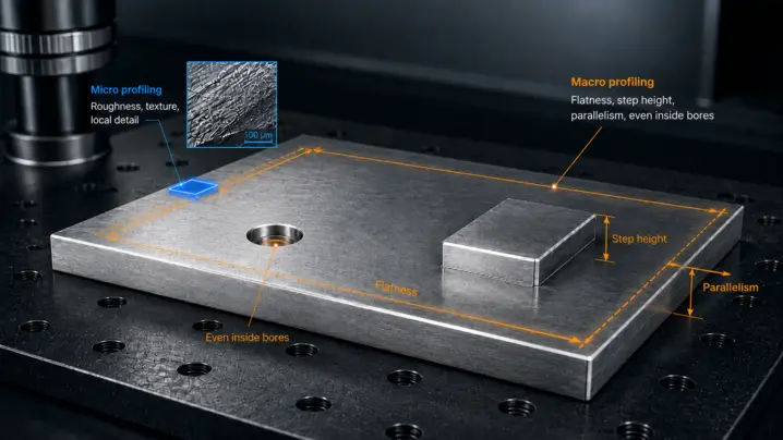
Pro.Surf inspects flatness, step height and parallelism on large parts and multi-part trays — non-contact, in seconds. No-crash telecentric optics measure even into bores, with the precision and repeatability production demands.
Metro.Lab
Metro.Lab is a compact, wide-area surface profiler. It combines high measurement performance with a small footprint—ideal for space or budget conscious applications that still require reliable 3D surface data.
Not sure which profiler fits your task? Two guides to help you decide.
Two short guides take you through the key decisions: one helps you choose the right measuring technology, the other the right measurement scale — micro or macro. And with our try-before-buy offer, you get the practical way to confirm your choice on your own parts.
Related applications and measurement tasks
Discuss your demands with our experts
Let’s start with a short discussion about your parts, tolerances, and workflow—and, if useful, we can add a feasibility study, PolyMeasure (contract measurements), or a PolyRent trial as optional next steps.