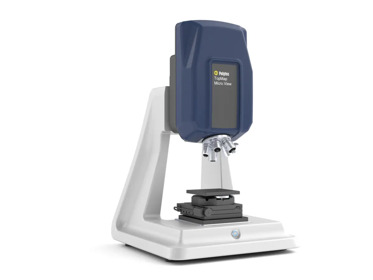
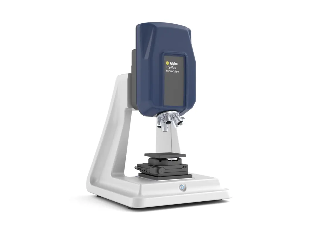
Most flexible and affordable system for 3D profiling with sub-nm precision
With an extended 100 mm Z measurement range and the CST Continuous Scanning Technology, Micro.View® measures complex (micro)topographies at nm resolution. This convenient table-top setup features integrated electronics, with the advanced Focus Finder simplifying and speeding up the measurement procedure.
- Reliable surface roughness analysis in sub-nm precision on various materials thanks to Smart Scanning Technology
- Widest and most variable FoV for flexible roughness analysis (from 0,07 x 0,05 mm up to 13,2 x 9,8 mm)
- True Stitching for unmatched accuracy of wider parts
- Wide Z measurement range of 100mm with full resolution due to Continuous Scanning Technology
- Recipe-driven measurement for repetitive operations
- Compliant to newest standards as ISO 25178, ISO 21920 and more
Micro.View specializes in high-resolution roughness and texture analysis whether for classic "line" profiling (Ra, Rz,...) or areal analysis (Sa, Sq,..). For applications with increased requirements for automation, serial measurements, or operator-independent workflows, we recommend Micro.View+ with a motorized turret, focus tracker, and advanced automation functions.
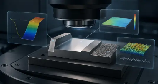
Easy 3D profiling of nearly any material, from detailed surface roughness to form and microstructure
Measure where others struggle
Many conventional optical profilers struggle with highly reflective, dark, low-contrast, or transparent materials. Micro.View overcomes this using embedded correlogram technology, which allows multiple scans at different light intensities. This enables reliable measurements even on complex materials.
The result: precise 3D data for topography, roughness, microstructures, step heights, and flatness — even on the most challenging surfaces. A key reason customers switch to Polytec is our ability to measure mirror-like or polished surfaces where other systems fail.
Precision by experience
With decades of experience, our engineers combined phase and envelope evaluation of the correlogram with inherently low system noise and our optional Environmental Compensation Technology (ECT). This results in sub-nanometer vertical resolution and outstanding 3D data clarity.
And with our True Stitching, using advanced algorithms (AI), our systems and software deliver an unmatched precision with wider samples.
This level of precision empowers engineers to verify tight tolerances, optimize production, and ensure long-term reliability.
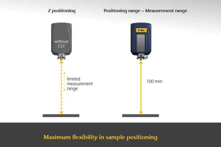
Utilizing the full Z-range
With Continuous Scanning Technology (CST), Micro.View uses the entire 100 mm travel range as usable Z-range — independent of the selected objective. This ensures stable resolution across tall parts and eliminates the need for repositioning.
Different stand options further support larger or taller samples, enabling flexible setup from small research parts to large industrial components.
Choose the right surface profiler with confidence—benefit from our "try before buy" approach.

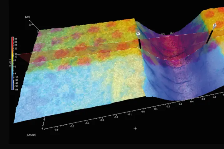
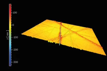
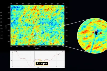
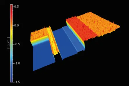
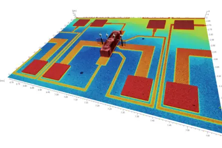
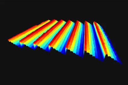
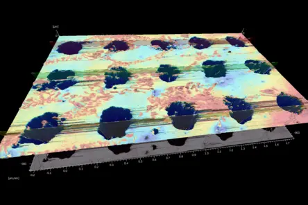
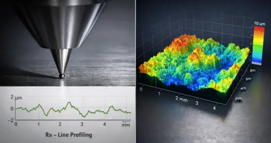
Examples of 3D surface roughness measurement with Micro.View profilers
Below or some real-life results from standard tasks, as measuring surface roughness (Ra, Rz, Sa, Sq,....) and form parameters, across common engineering materials. Those examples are gathered by our application centers which does feasibility studies and offers contractual measurement services.

Choose the right surface profiler with confidence—talk to our metrology experts.
Rich feature set for surface roughness in lab or production
With an extended 100 mm Z measurement range and the CST Continuous Scanning Technology, Micro.View measures complex topographies at nm resolution. This convenient table-top setup features integrated electronics, with the advanced Focus Finder simplifying and speeding up the measurement procedure.
True Stitching - Higher accuracy for wider samples
Because larger surfaces exceed the single-shot field of view — stitching merges tiles into one accurate dataset. The metrology quality of such large-area measurements depends on the optics and sensing technology, the number of tiles and the stitching algorithms.
True Stitching delivers high-fidelity large-area measurements by minimizing stitching artifacts and preserving geometry.
An independent benchmarking at a leading German technical university compared six optical profilers from different manufacturers and the Polytec profilometer demonstrated the highest stitching and measurement quality. This is achieved by various features as:
- Large single-shot FoV → fewer tiles and seams, less cumulative error
- Sophisticated stitching algorithms → controlled overlap, robust registration, and metrology-safe blending that preserves steps and edges
The result is high-fidelity, large-area topography with fewer artifacts and audit-ready residuals—what we call True Stitching.
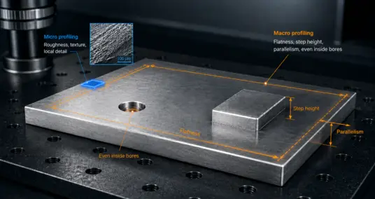
Sub-nm surface roughness inspection with large FoV
Widest Field of View - up to 13,2 x 9,8 mm
The new and unique 0.6x lens literally expands your view: Micro.View allows the analysis of high-resolution surface roughness, texture or microstructures using classic 20x to 111x. A single click with automatic lens switch to 0.6x allows for a seemless transition to large-area form or flatness measurements. Examine microstructures on large scale without stitching. Reveal all structural details while keeping an eye on form parameters, warpage or large area steps.
CSI – coherence scanning interferometry for highest precision.
Micro.View is based on CSI (also called white-light interferometry), the industry standard for non-contact, areal surface metrology. It scans a broadband light source vertically and analyzes the interference pattern.
- Envelope evaluation: robust on rough and low-contrast surfaces
- Phase evaluation: sub-nanometer resolution on smooth, flat samples
- Correlogram analysis: full use of the interference pattern for maximum robustness and accuracy
This allows measurement of both polished optics and rough technical parts with the same system.
CST – full 100 mm Z-range without sacrificing resolution.
Continuous Scanning Technology (CST) transforms the entire 100 mm travel range into usable Z-range with consistent resolution — independent of lens.
- Supports large and tall samples without repositioning
- Maintains accuracy throughout the measurement range
- Reduces setup effort and avoids stitching or refocusing
ECT – stable 3D surface data on the shop floor.
Noise, vibration, and temperature fluctuations can affect measurements. Our Environmental Compensation Technology (ECT) compensates for such disturbances and ensures consistent data — even on the shop floor.
- Improves reliability in noisy or unstable environments
- Enables automation and inline QC without full isolation
- Especially helpful for sensitive components (e.g., MEMS, thin films)
Focus Finder and recipe management for fast and reliable measurements
Accurate focus is critical for surface metrology. With the implemented Focus Finder the system automatically detects optimal focus point to reduce setup time and enables reliable recipe measurements.
With the easy to use and select recipe management and optional barcode reader measurements can be selected and run easily and reproducible.
ECT and CST
Environment Compensation and Continues Scanning Technology to support easy and unattended measurements
Smart Scanning Technology
SST supports measurement of reflective or matte surfaces
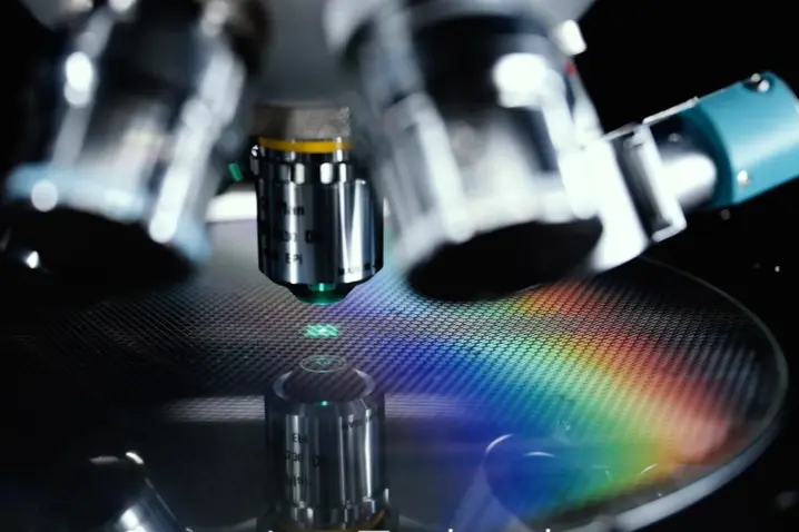
5-lense turret
Quick switching of lenses for different metrology tasks and components
100mm Z-Range (and more)
100mm z-range (equals measurement range) with Continuous Scanning Technology (CST).
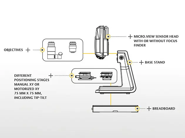
Modular setup and specification for 3D profiling
| Z Range | 100 mm (positioning & measurement) |
| Vertical resolution | 0.01 nm |
| Repeatability of RMS | 0.05 nm |
| Sample reflectivity | 0.05 to 100 % |
| Measuring points X-Y pixels | 1.352.000 (effective pixels) 1.352 x 1000 |
| Measuring speed | 100 µm/s |
| ISO parameters | ISO 25178, ASME B46.1, ISO 4287, ISO 13565, ISO 21920 |

Feasibility check?
Send us your sample and we run a feasibility study with our profiler and walk with your through the results.
This gives you a precise understanding of the optical profiler’s performance on your actual samples.
Related information and downloads
Stylus or optical profiler
Learn when non-contact 3D metrology offers clear advantages over tactile measurement — from speed and flexibility to delicate surface inspection.
Micro or macro 3D profiling?
Find out how measurement scale, sample size and application requirements influence the choice of the right optical surface profiler.
Which optical profiler technology is the right one?
Compare key technologies such as WLI, confocal microscopy and focus variation — and understand which method best fits your surface.
Downloads
Discuss your demands with our experts
Let’s start with a short discussion about your parts, tolerances, and workflow—and, if useful, we can add a feasibility study, PolyMeasure (contract measurements), or a PolyRent trial as optional next steps.