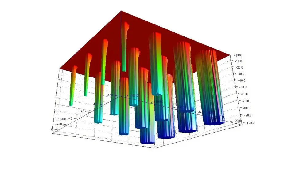
Characterizing vertical interconnect accesses (VIA)
Vertical electrical connections – also known as “vertical interconnect accesses” or VIAs for short – are mainly used in high-density, integrated switching circuits and have structures with a high aspect ratio. TSVs (through silicon VIAs) in particular have become an established technology in the semiconductor segment.
Polytec's optical surface metrology allows easy and reliable quality inspections: check etching depths in automated processes, measure distances and surface parameters on VIA. Chromatic confocal sensors and microscope-based profilers offer versatile measurement capabilities, for both in the laboratory and at production level and inline.
Fitting surface profilers
Roughness Tester
The Roughness Tester is our entry Micro.View system and the most cost effective way to get started into the 3D surface roughness measurement. Step from R to S parameters.
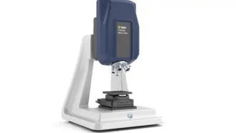
Micro.View
TopMap Micro.View® is an easy to use optical profiler in a compact table-top setup. Choose Micro.View® as the cost-effective inspection tool for examining precision-engineered surfaces down to the sub-nm range, for inspecting roughness, microstructures and more surface details.
Micro.View+
Advanced microscope-based surface profiler with automation and color imaging. Micro.View+ enables repeatable, operator-independent roughness and texture analysis—ready for lab and production use.
Choose the right surface profiler with confidence—benefit from our "try before buy" approach.
Fitting application and measurement tasks
Discuss your demands with our experts
Let’s start with a short discussion about your parts, tolerances, and workflow—and, if useful, we can add a feasibility study, PolyMeasure (contract measurements), or a PolyRent trial as optional next steps.