Keep layer thickness constant to minimize quality costs
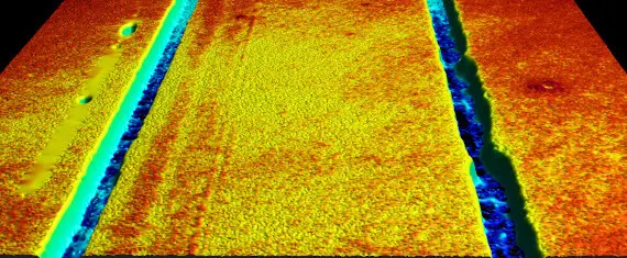
The material thickness of transparent surfaces and layers is critical for both their fitting accuracy and function in surface metrology. Inspecting layer thickness along the production process by performing measurements and constantly maintaining the exact same level is indispensable if high quality and a low rejection rate are to be achieved. If your job involves performing an areal analysis of how thick a transparent sample is or in detecting surface defects, then Polytec’s TopMap series is perfect for you.
A major consideration for most coating processes is that the coating is applied at a controlled and defined thickness. Coating technologies include composite coatings, nano coatings and ultra-thin films, deposition (plasma and ion-based vacuum), epitaxial film growth, sputter technologies, dip, flow and spin coatings, spraying, painting and rolling, electroplating and electroless plating, and or surface modification.
Control layer thickness and the entire coating process
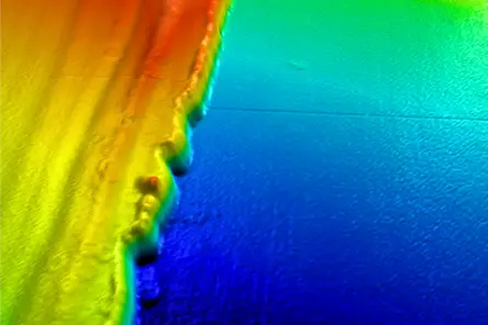
The scratch test is a popular adhesion test for thin, hard and well-adhering coatings such as TiC (titanium carbide) on steel or cemented carbide substrates. Coating thickness measurement of non-transparent materials can also be measured at the edge of a coating or by a step-height measurement of the scratch. Layer thicknesses from a few μm upwards can be detected on transparent coatings at any position.
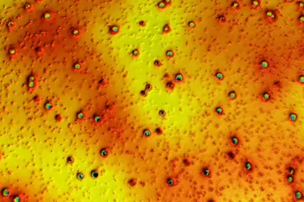
A wide variety of surface defects in coating and metallizing can be measured, qualified and catalogued, including voids, streaks, chatter, droplets, spots, dimples, holes, scratches, coating disturbances, contaminants, orange peel, and visual texture appearance. Defects can be quickly visualized, measured and the information used to help identify its cause, so that process cures can be quickly implemented, optimized and then monitored to show the improvements in end coated surface quality control. Defects can be measured and qualified on a coating to help identify the cause.
As an example, Polytec’s surface measurement systems are used to check and maintain the thickness of cell phone displays during production.

Related products
Roughness Tester
The Roughness Tester is our entry Micro.View system and the most cost effective way to get started into the 3D surface roughness measurement. Step from R to S parameters.
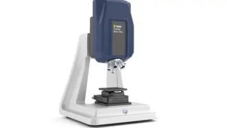
Micro.View
TopMap Micro.View® is an easy to use optical profiler in a compact table-top setup. Choose Micro.View® as the cost-effective inspection tool for examining precision-engineered surfaces down to the sub-nm range, for inspecting roughness, microstructures and more surface details.
Micro.View+
Advanced microscope-based surface profiler with automation and color imaging. Micro.View+ enables repeatable, operator-independent roughness and texture analysis—ready for lab and production use.
Choose the right surface profiler with confidence—benefit from our "try before buy" approach.

Further surface parameters
Surface texture
Surface texture defines a material's topography regarding roughness, waviness & lay.
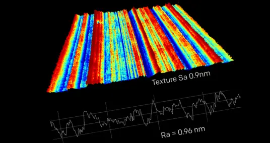
Surface roughness
Learn what surface roughness is, how Ra, Rz, Sa and Sq are defined and which standards apply when.
Surface flatness measurement
Measure surface flatness and characterize workpiece topography regarding surface flatness tolerances according to ISO 1101, ISO 12781
Surface step height
Profilometric step-height measurement delivers objective layer/etch depth and uniformity from areal data, supporting ISO-aligned reporting and production SPC.
Discuss your demands with our experts
Let’s start with a short discussion about your parts, tolerances, and workflow—and, if useful, we can add a feasibility study, PolyMeasure (contract measurements), or a PolyRent trial as optional next steps.