垂直相互接続アクセス(VIA)の特性評価
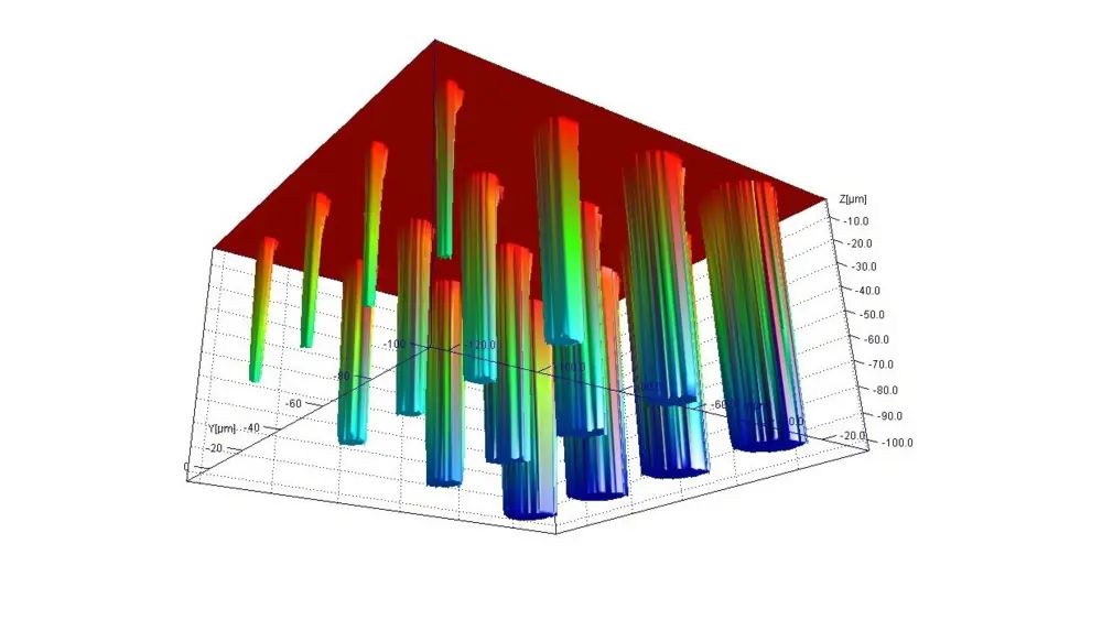
垂直電気接続(別名「垂直相互接続アクセス」、略称VIA)は、主に高密度集積スイッチング回路に使用され、アスペクト比の高い構造を有します。特にTSV(貫通シリコンビア)は半導体分野で確立された技術となっています。
Polytec光学表面計測技術により、容易かつ信頼性の高い品質検査が可能:自動化プロセスにおけるエッチング深さの確認、VIA上の距離や表面パラメータの測定。色差共焦点センサーと顕微鏡ベースのプロファイラーは、実験室レベルから生産ライン内(インライン)まで、多様な測定能力を提供します。
表面プロファイラーの取り付け
Micro.View
TopMap Micro.View® is an easy to use optical profiler in a compact table-top setup. Choose Micro.View® as the cost-effective inspection tool for examining precision-engineered surfaces down to the sub-nm range, for inspecting roughness, microstructures and more surface details.
Micro.View+
Advanced microscope-based surface profiler with automation and color imaging. Micro.View+ enables repeatable, operator-independent roughness and texture analysis—ready for lab and production use.
自信を持って最適な表面プロファイラーをお選びください——「購入前に試用」という当社のアプローチのメリットを享受いただけます。