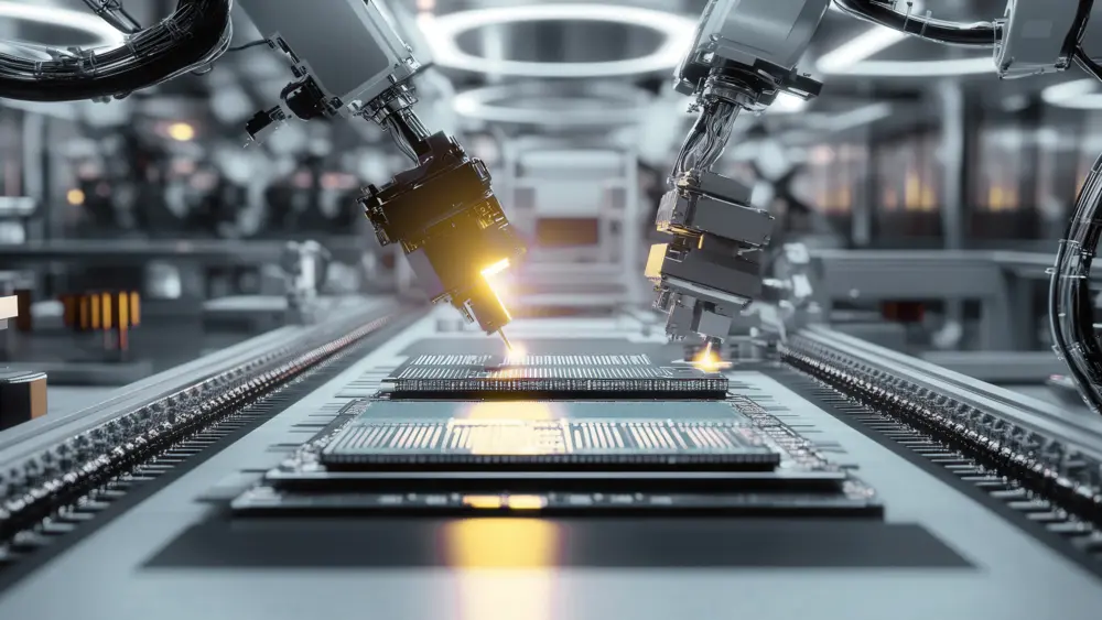
Characterizing microsystems' and MEMS' topography and dynamics
Using the versatile surface measurement systems from Polytec, you can complete your micro- and nanotechnology tasks reliably, quickly, and with a high level of precision. You can measure channel depths on your lab-on-a-chip, determine step height on MEMS packaging, establish how flat pressure sensors are and characterize MEMS using surface parameters. Even performing dynamic out-of-plane and in-plane measurements on RF filters to determine MHz resonance frequencies will be a simple task for you now — thanks to Polytec’s MSA Micro System Analyzer series.
Related applications
MEMS pressure sensor
Surface characterization of MEMS pressure sensors for optimal quality & production control. Explore more about measuring MEMS pressure sensors.
Vertical interconnect access (VIA)
Reliable quality inspections: check etching depths in automated processes, measure distances and surface parameters on Vertical interconnect accesses.
Flexible electronics
Polytec optical systems ensure process control and tolerance checks in printed and in-foil hybrid electronics with integrated chips
Die bonding
In epoxy die bonding, the accurate placement & attachment of the die is crucial for quality. Ask for TopMap surface metrology for die bonding process control.
Lab-on-a-chip
Test your lab-on-a-chip devices (LoC) using 3D measurement data evaluating form parameters for quality control: channel depth, step height and flatness.
Related measurement tasks
Coating Quality Control in 3D
Coating quality control in 3D. Assessing pre-coat texture, post-coat defects, and film thickness.
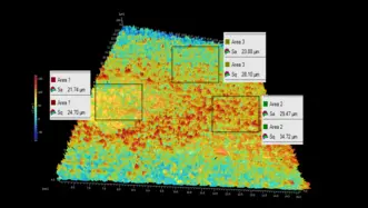
Surface roughness measurement
Surface texture analysis in 3D. From Sa/Sq to Str/Sal for validating specifications and surface features.
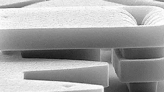
Surface metrology on microstructures
Topography & dynamics of microstructures and for nanotech. 3D geometry, roughness, and time-resolved motion.
Optical profilers and vibrometers for micro- and nanotechnology
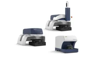
Macro Profiler
Pro.Surf inspects flatness, step height and parallelism on large parts and multi-part trays — non-contact, in seconds. No-crash telecentric optics measure even into bores, with the precision and repeatability production demands.
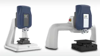
Micro Profiler
Micro.View profiler systems are optimized for measurements with sub-nanometer resolution. With focused optics and high vertical resolution they enable detailed analysis of microstructures, surface finish and material distribution where even the smallest deviations matter.
Microscope-based vibrometers
Inspired by the rapid further development of microelectromechanical systems and MEMS, Polytec presents this highly innovative product line of microscope-based measurement systems. MSA Micr System Analyzers from Polytec validate dynamics and topography of microsystems reliably with utmost precision.
Discuss your demands with our experts
Let’s start with a short discussion about your parts, tolerances, and workflow—and, if useful, we can add a feasibility study, PolyMeasure (contract measurements), or a PolyRent trial as optional next steps.