マイクロシステムおよびMEMSの地形と動的特性の評価マイクロシステムおよびMEMSのトポグラフィーとダイナミクスの特性評価
Polytec の多機能表面測定システムを使用すれば、マイクロ・ナノテクノロジーの課題を信頼性高く、迅速に、高精度で遂行できます。 ラボオンチップ上のチャネル深さの測定、MEMSパッケージングにおける段差高さの判定、圧力センサーの平坦度評価、表面パラメータを用いたMEMS解析が可能です。さらに、RFフィルターの動的面外・面内測定によるMHz単位の共振周波数測定も、Polytecの MSAMicro System Analyzer シリーズにより、今や簡単な作業となります。
関連アプリケーション
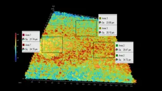
MEMS圧力センサー
Surface characterization of MEMS pressure sensors for optimal quality & production control. Explore more about measuring MEMS pressure sensors.
垂直相互接続アクセス(VIA)
Reliable quality inspections: check etching depths in automated processes, measure distances and surface parameters on Vertical interconnect accesses.
フレキシブルエレクトロニクス
Polytec optical systems ensure process control and tolerance checks in printed and in-foil hybrid electronics with integrated chips
ダイボンディング
In epoxy die bonding, the accurate placement & attachment of the die is crucial for quality. Ask for TopMap surface metrology for die bonding process control.
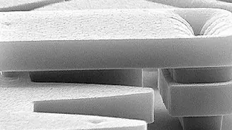
ラボ・オン・ア・チップ
Test your lab-on-a-chip devices (LoC) using 3D measurement data evaluating form parameters for quality control: channel depth, step height and flatness.
関連する測定タスク
マイクロ・ナノテクノロジー向け光学プロファイラーおよび振動計
マクロプロファイラ
Pro.Surf は、大型部品やマルチパートトレイの平面度・段差・平行度を非接触でわずか数秒で検査します。衝突を防ぐテレセントリック光学系は穴の内部まで測定でき、生産現場が求める精度と再現性を実現します。
マイクロプロファイラー
Micro.View systems are optimized for ultra-high-resolution measurements in the sub-nanometer range. With focused optics and high vertical resolution they enable detailed analysis of microstructures, surface finish and material distribution where even the smallest deviations matter.
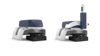
顕微鏡型レーザドップラ振動計
ポリテックのマイクロシステムアナライザは、MEMSのダイナミクスと形状の両方を測定することができる理想的な顕微鏡型システムです。 MEMSなどの電子デバイスは、電気テストで、デバイスが動作しているかどうかは証明できますが、デバイスがどう動作しているか、その正確な動きを見るには、レーザドップラ振動計しか手段がありません。また、小型軽量化、高周波駆動化する昨今では、非接触測定が可能で、かつ、キロヘルツ、メガヘルツ、さらにギガヘルツの高周波帯域でも、ナノピコ分解能で高精度に振動変位を測定できるレーザドップラ振動計は、必須のテスティングツールであると言えます。 さらにマイクロシステムのダイナミクスだけでなく形状もナノメートル精度で測定します。伝達関数の測定はもちろん、マイクロシステムの静的および動的な 3D 特性評価、Si 封止MEMSの測定、(真空)プローブステーションへの統合が可能な、ユニークなオールインワンソリューションです。