
微系统和MEMS的拓扑结构与动力学特性表征
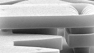
借助Polytec 提供的多功能表面测量系统,您可以可靠、快速且高精度地完成微纳米技术相关任务。 您可以测量芯片实验室上的通道深度,测定MEMS封装的台阶高度,评估压力传感器的平整度,并利用表面参数对MEMS进行表征。如今,即使是对射频滤波器进行动态的离平面和面内测量以确定兆赫兹(MHz)级谐振频率,对您来说也变得轻而易举——这都要归功于Polytec的 MSA显微式激光测振仪系列。
用于微纳米技术的光学轮廓仪和激光测振仪
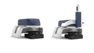
大视场三维光学轮廓仪
Pro.Surf 可对大型工件及多样本料盘进行平面度、台阶高度与平行度检测——非接触、数秒完成。防碰撞远心光学系统可深入深孔内部进行测量,满足生产环节对精度与重复性的严苛要求。
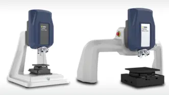
三维光学轮廓仪
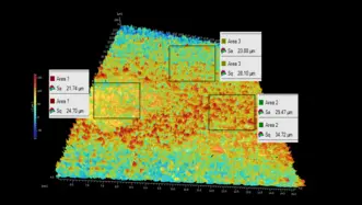
Micro.View 系列三维光学轮廓仪专为亚纳米级分辨率测量而优化。凭借聚焦光学系统与高垂直分辨率,可对微观结构、表面光洁度及材料分布进行精细分析——在最微小的偏差都可能影响性能的场景中,提供可靠的数据支撑。
显微式激光测振仪
随着微机电系统和MEMS快速发展,Polytec推出了高度创新的显微式测量系统产品线。Polytec的MSA系列显微式激光测振仪带宽可达数kHz,数MHz,甚至数GHz,以最高精度可靠地验证微系统的动力学特性和轮廓数据。MSA集多功能于一体,可用于确定传递函数、表征微器件的3D静态和动态特性,甚至可透过封装好的硅帽,获取其在工作条件下的整个层制结构。