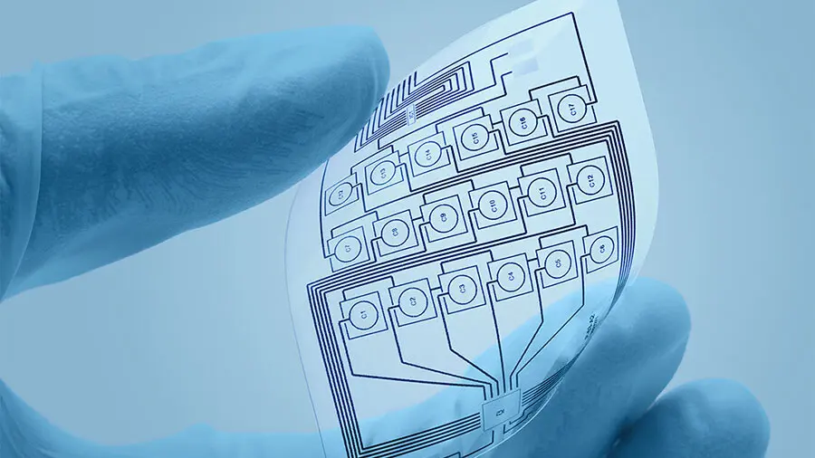
Characterizing flexible electronics in 3D
Flexible electronics open up a realm of new applications in the fields of wearables, thin film solar cells, RFIDs and displays used in automotive dashboards or medical applications. For all these use cases, the product reliability is a key quality indicator. Also there is an increasing demand in components to be harmonized for signal processing, communication and energy generation.
For such applications, white-light interferometry allows scanning the entire surface of hybrid flexible electronics in a single shot. The optical and non-destructive measurement method characterizes printed electronics on behalf of form parameters, roughness and structural details and help secure the electronics quality and functionality.
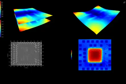
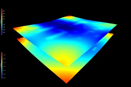
Form parameters & surface roughness of printed electronics
Scanning surfaces and evaluating 3D height information enables a fast and reliable characterization of printed and flexible electronics. 3D surface metrology solutions from Polytec provide meaningful data for both electronics quality and printed electronics process stability. The advanced color information mode helps determining and localizing defects.
For in-line integration and for semi- or fully automated manufacturing processes of flexible electronics, TopMap sensor heads can easily be integrated into production lines, offering customized solutions for in-line inspection. Upon demand, users can manage and load predefined measurement settings, enabling one-click inspections at production level using measurement recipes. Our PolyXperts are happy to assist at all project stages, such as developing custom routines and evaluations, using the open software architecture.

Characterziation of micro electronics
Fitting surface profiler
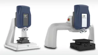
Micro Profiler
Micro.View profiler systems are optimized for measurements with sub-nanometer resolution. With focused optics and high vertical resolution they enable detailed analysis of microstructures, surface finish and material distribution where even the smallest deviations matter.
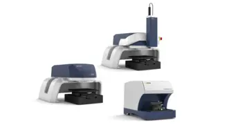
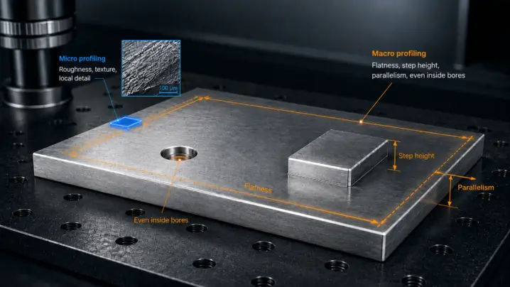
Macro Profiler
Pro.Surf inspects flatness, step height and parallelism on large parts and multi-part trays — non-contact, in seconds. No-crash telecentric optics measure even into bores, with the precision and repeatability production demands.
Metro.Lab
Metro.Lab is a compact, wide-area surface profiler. It combines high measurement performance with a small footprint—ideal for space or budget conscious applications that still require reliable 3D surface data.
Not sure which profiler fits your task? Two guides to help you decide.
Two short guides take you through the key decisions: one helps you choose the right measuring technology, the other the right measurement scale — micro or macro. And with our try-before-buy offer, you get the practical way to confirm your choice on your own parts.
Related applications and measurement tasks
Discuss your demands with our experts
Let’s start with a short discussion about your parts, tolerances, and workflow—and, if useful, we can add a feasibility study, PolyMeasure (contract measurements), or a PolyRent trial as optional next steps.