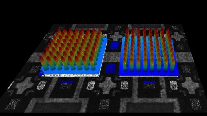
Optical inspection of PCB and BGA
The reliability of PCB and the respective PCB components like IC (integrated circuit) or BGA (ball grid array) can vary with every design and selection of semiconductor components installed. For each type and series of PCB design, ideally automated, in-process quality control and testing of PCB is needed at manufacturing.
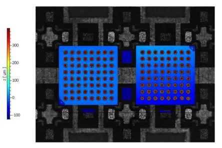
In addition, at customer level for inspecting for “dead on arrival” issues, caused for example by breaking on weak points during transportation, quality control methods are part of the process. TopMap optical 3D surface metrology allow fast scanning of entire sample surfaces with nanometer resolution, providing areal topography data of PCB, IC and BGA in a single shot.
Types of ball grid array packaging
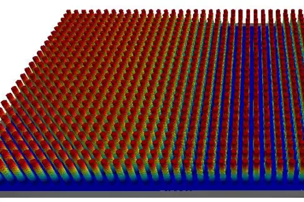
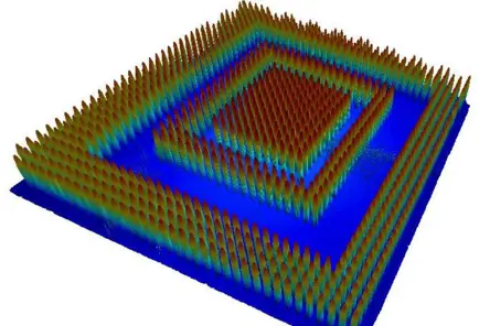
Looking onto the history of semicon packaging, there were DIPs (dual in line package) at first, QFP (quad flat package) or QFN (quad flat no leads), BGA (ball grid arrays) as one of the most popular packaging techniques, leading to the always higher pin count. BGA are well established in consumer electronics such as smartphones, tablets, motherboards and digital cameras. In comparison to DIPs and QFPs: the BGA shows more I/O connections, shorter connectors leading to improved performance and high speed. Bump materials typically are SnPb , SnAgCu , SnIn, SnBi with bump diameters typically reaching 90-400 µm and a distance between bumps of around 0.1 to 2 mm.
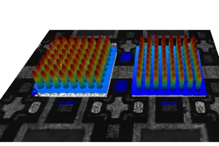
Typical failure and defects in BGA manufacturing
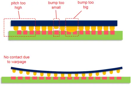
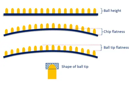
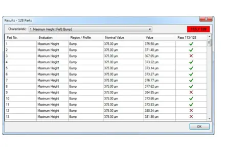
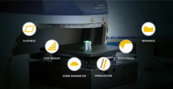
In the manufacturing of BGAs, for example using the flip chip method, which describes the connection by applying heat and pressure on the substrate, typical manufacturing errors or defects can occur when the pitch is too high or the bump is too small or too big. Polytec TopMap surface profilers are ideal metrology solutions for areal measurement and inspection of ball height / bump height, coplanarity, chip flatness and chip warpage, bga ball flatness, for optical inspection of the entire BGA pitch or focusing on the shape of the pure ball tip in an optical and non-contact way.
Choose the right surface profiler with confidence—let us run a feasibility study with your sample.

BGA warpage & quality control
In the manufacturing of BGAs, for example using the flip chip method, which describes the connection by applying heat and pressure on the substrate, typical manufacturing errors or defects can occur when the pitch is too high or the bump is too small or too big. Polytec TopMap surface profilers are ideal metrology solutions for areal measurement and inspection of ball height / bump height, coplanarity, chip flatness and chip warpage, bga ball flatness, for optical inspection of the entire BGA pitch or focusing on the shape of the pure ball tip in an optical and non-contact way.
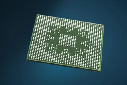
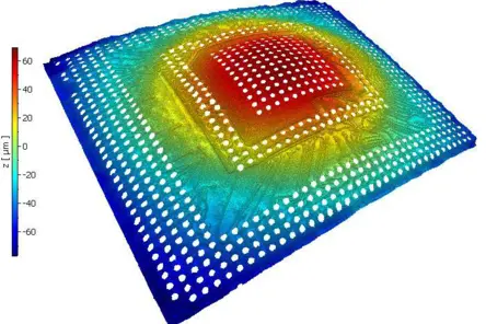
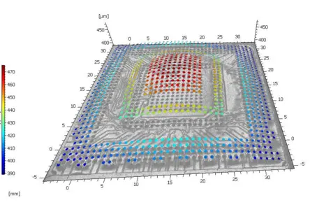
3D profiling as quality inspection of ball grid arrays
Areal optical 3D profiling is a powerful tool for quality inspection of electronic assemblies. It supports, among other things:
- inspection of printed circuit boards (PCBs) and BGAs
- analysis of flatness, coplanarity, and height distributions
- pass/fail evaluations in production
- failure analysis in the event of defects and process deviations
Especially in multilayer PCB structures, precise layer thickness measurement is becoming increasingly important. Optical inspection solutions from Polytec provide reproducible measurement data for this purpose and enable targeted process feedback.
Surface profiler for BGA and semiconductor measurement
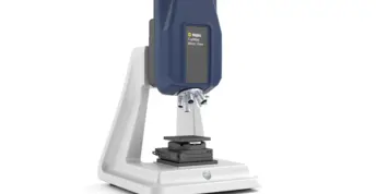
Micro.View
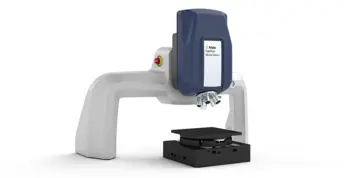
TopMap Micro.View® is an easy to use optical profiler in a compact table-top setup. Choose Micro.View® as the cost-effective inspection tool for examining precision-engineered surfaces down to the sub-nm range, for inspecting roughness, microstructures and more surface details.
Micro.View+
Advanced microscope-based surface profiler with automation and color imaging. Micro.View+ enables repeatable, operator-independent roughness and texture analysis—ready for lab and production use.
Choose the right surface profiler with confidence—benefit from our "try before buy" approach.

Related applications and measurement tasks

Discuss your demands with our experts
Let’s start with a short discussion about your parts, tolerances, and workflow—and, if useful, we can add a feasibility study, PolyMeasure (contract measurements), or a PolyRent trial as optional next steps.