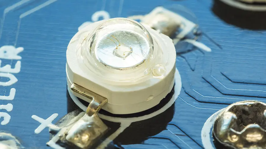
Capturing HPLDs in a single pass
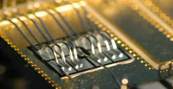
To guarantee that high-power laser diodes (HPLDs) will work reliably, it is important to check that the enclosure has the correct flatness and step height levels. To do this, you should use tried-and-tested technology that captures the smallest of height differences and that gives you measurement results reliably and quickly. We are, of course, talking about the surface measurement systems from Polytec.
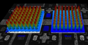
TopMap optical 3D surface metrology systems allow the characterization of diodes in laser arrays in a large field-of-view and areal measurement, analyzign both the “smile” surface curvature and step heights directly on semiconductors. The large field of view captures all details in one measurement, leading to convenient, comprehensive and efficient inspections of the laser diodes’ enclosure without sacrificing high resolution.
Surface profiler for diodes and electronic components
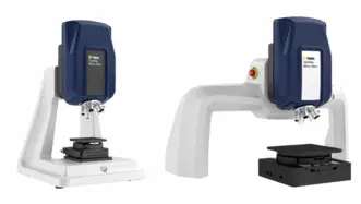
Micro-Profiler
Micro.View profiler systems are optimized for measurements with sub-nanometer resolution. With focused optics and high vertical resolution they enable detailed analysis of microstructures, surface finish and material distribution where even the smallest deviations matter.
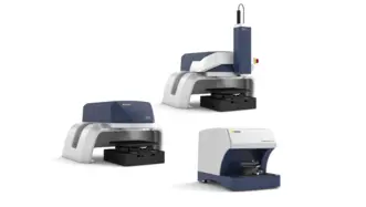
Macro Profiler
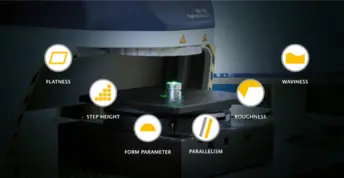
Pro.Surf inspects flatness, step height and parallelism on large parts and multi-part trays — non-contact, in seconds. No-crash telecentric optics measure even into bores, with the precision and repeatability production demands.
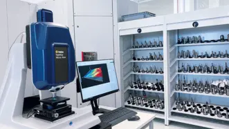
Roughness Deal Days
Save 30% on Polytec’s optical Roughness Tester—precise, non-contact 3D profilometry with sub-nm resolution. Offer valid until October 31, 2026.
Related applications and measurement tasks

Discuss your demands with our experts
Let’s start with a short discussion about your parts, tolerances, and workflow—and, if useful, we can add a feasibility study, PolyMeasure (contract measurements), or a PolyRent trial as optional next steps.