Surface topography of electronics, semiconductors and solar technology
You can ideally adapt Polytec’s versatile solutions in the semiconductor industry for your applications in the electronics and solar technology industries. In the field of software, for example, you can do so by utilizing application-specific user interfaces for the OK / NOK analysis. Polytec offers you solutions to check electronic contacts — both for analyzing the height of BGAs or “solder bumps” and for analyzing the co-planarity of IC pins. You’ll also find the right systems for packaging high-power laser diodes at Polytec.
Optical profilers and vibrometers for eletronics and semiconductor industry
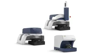
Macro Profiler
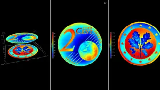
Pro.Surf inspects flatness, step height and parallelism on large parts and multi-part trays — non-contact, in seconds. No-crash telecentric optics measure even into bores, with the precision and repeatability production demands.
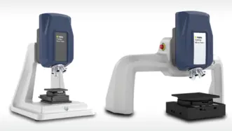
Micro Profiler
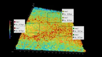
Micro.View profiler systems are optimized for measurements with sub-nanometer resolution. With focused optics and high vertical resolution they enable detailed analysis of microstructures, surface finish and material distribution where even the smallest deviations matter.
Microscope-based vibrometers
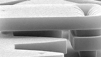
Inspired by the rapid further development of microelectromechanical systems and MEMS, Polytec presents this highly innovative product line of microscope-based measurement systems. MSA Micr System Analyzers from Polytec validate dynamics and topography of microsystems reliably with utmost precision.
Choose the right surface profiler with confidence—benefit from our "try before buy" approach.

Discuss your demands with our experts
Let’s start with a short discussion about your parts, tolerances, and workflow—and, if useful, we can add a feasibility study, PolyMeasure (contract measurements), or a PolyRent trial as optional next steps.