電子機器、半導体及び太陽電池技術における表面形状
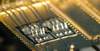
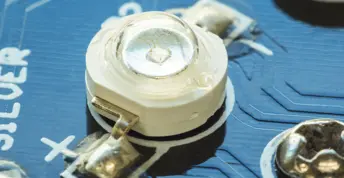
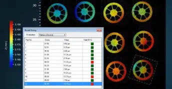
Polytecの半導体産業向け多機能ソリューションは、電子機器や太陽電池技術産業におけるお客様の用途に最適に適合させることが可能です。例えばソフトウェア分野では、OK/NOK分析用のアプリケーション特化型ユーザーインターフェースを活用することで実現できます。Polytec は電子接点の検査ソリューションを提供します。BGAや「はんだバンプ」の高さ分析からICピンのコプラナリティ分析まで対応可能です。Polytec では、高出力レーザーダイオードのパッケージングに適したシステムもご提供しています。
Surface metrology for semiconductors and electronics
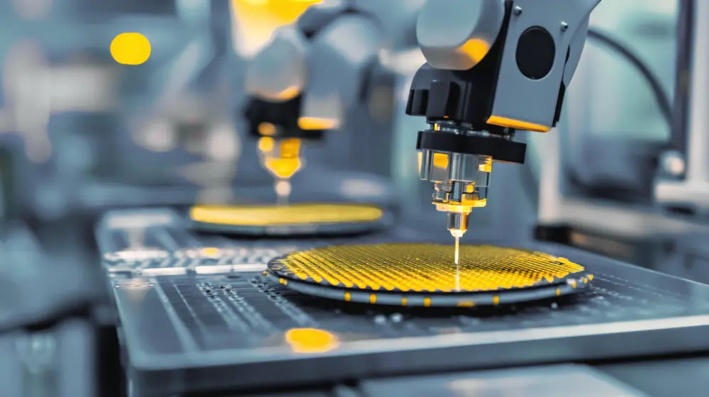
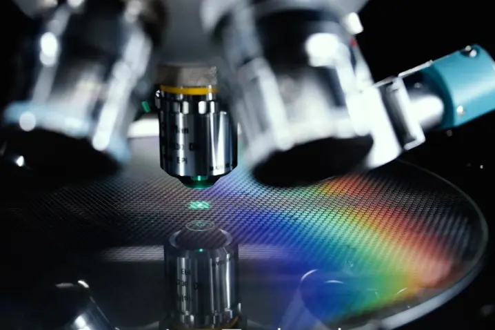
With semiconductor devices becoming smaller and packaging technologies becoming increasingly complex, Semicon & electronic manufacturing requires non-contact, nanometer-precision surface metrology throughout the production process. TopMap white-light interferometry (WLI) provides fast, highly precise 3D measurements of surfaces without risk of collision or damage to the surface structures.
TopMap profilers offer measurement solutions for wafers, MEMS, advanced packaging and electronics, providing reliable quality control, process optimization, and failure analysis with nanometer resolved topography, step height, roughness, flatness, bow & warpage or thickness measurements.
Semiconductor applications for TopMap 3D profilers
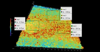
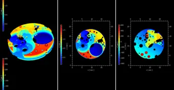
- Measure silicon wafers, check wafer flatness, characterize bow and warp characterization or surface waviness including wafer roughness after CMP.
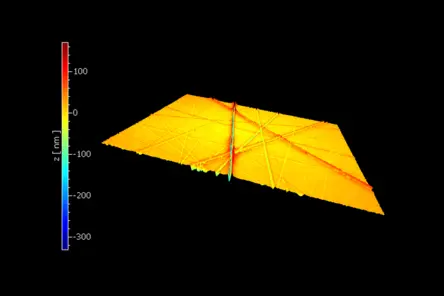
- Chemical-mechanical polished wafers (CMP surfaces), inspecting for remaining step height, scratch and defect detection, surface roughness after polishing
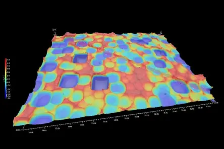
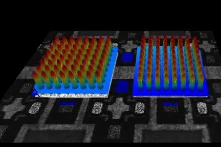
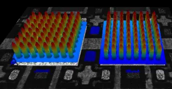
- Inspect micro-bumps and solder bumps in regard of the bump height, coplanarity and roundness of pins
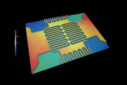
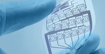
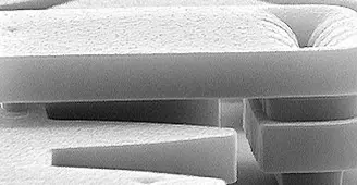
- Deformation on MEMS and micro electronics, micro-mirror flatness, surface roughness or etching depth
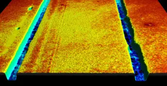
- Inspect depth of TSVs and diameter of VIAs, including measurements on recessed areas or surface planarity around VIAs.
- and more

電子・半導体産業向け光学プロファイラーおよび振動計
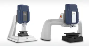
マイクロプロファイラー
Micro.Viewシステムは、サブナノメートル領域の超高分解能測定向けに最適化されています。集光光学系と高い高さ分解能により、微細構造、表面仕上げ、材料分布を詳しく解析できます。わずかな偏差も見逃せない用途に適しています。
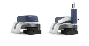
マクロプロファイラ
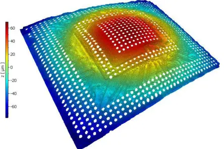
Pro.Surf は、大型部品やマルチパートトレイの平面度・段差・平行度を非接触でわずか数秒で検査します。衝突を防ぐテレセントリック光学系は穴の内部まで測定でき、生産現場が求める精度と再現性を実現します。
顕微鏡型レーザドップラ振動計
ポリテックのマイクロシステムアナライザは、MEMSのダイナミクスと形状の両方を測定することができる理想的な顕微鏡型システムです。 MEMSなどの電子デバイスは、電気テストで、デバイスが動作しているかどうかは証明できますが、デバイスがどう動作しているか、その正確な動きを見るには、レーザドップラ振動計しか手段がありません。また、小型軽量化、高周波駆動化する昨今では、非接触測定が可能で、かつ、キロヘルツ、メガヘルツ、さらにギガヘルツの高周波帯域でも、ナノピコ分解能で高精度に振動変位を測定できるレーザドップラ振動計は、必須のテスティングツールであると言えます。 さらにマイクロシステムのダイナミクスだけでなく形状もナノメートル精度で測定します。伝達関数の測定はもちろん、マイクロシステムの静的および動的な 3D 特性評価、Si 封止MEMSの測定、(真空)プローブステーションへの統合が可能な、ユニークなオールインワンソリューションです。
自信を持って最適な表面プロファイラーをお選びください——「購入前に試用」という当社のアプローチのメリットを享受いただけます。

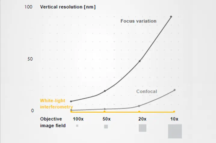
Why use white-light interferometry for semicon & electronics
White-light interferometry combines exceptional vertical resolution with fast, non-contact measurements. Guided workflows in the Sherpa software help automate, speed up procedures, while high-repeatability and valid measurement results comply with cycle times and demands of higher throughput. Compared with tactile profilometers or conventional optical microscopes, TopMap white-light interferometers deliver more insights in less time.