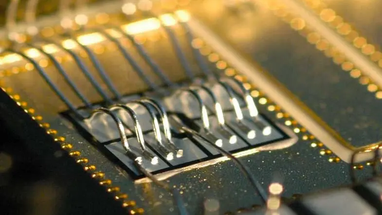
Control epoxy die bonding by surface characterization
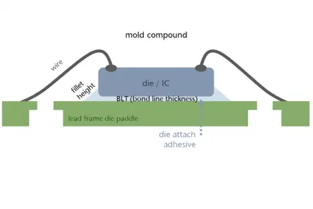
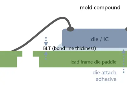
In epoxy die bonding and related die attach processes, even small deviations can affect process stability, component reliability, and lifetime. Key quality indicators such as bond line thickness (BLT), die tilt, and positioning accuracy must, therefore, be monitored reliably and repeatably.
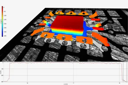
Polytec’s TopMap optical surface profilers enable fast, non-contact inspection of epoxy die bonding processes. They provide precise 3D surface data for automated quality control — from die orientation and tilt to bond line thickness — directly in production environments.
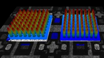
Characterizing QFN packages (quad-flat no-leads)
TopMap 3D surface metrology solutions integrate easily into production lines and deliver automated, high-resolution in-process measurements for epoxy die bonding. Typical inspection tasks include:
- Die tilt and die positioning
- Bond line thickness (BLT) and BLT height
- Torsion and relative positioning to reference features
In QFN packages, the die attach fillet — the adhesive excess rising along the die edges — plays a key role in mechanical stability. Based on precise BLT measurements, relevant parameters such as fillet width, height, and slope angle can be evaluated and optimized to improve process robustness and component quality.
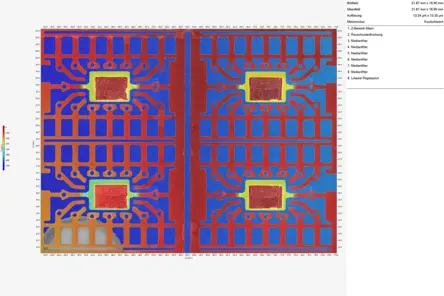
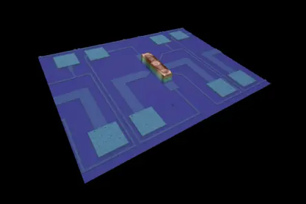
Bond line thickness, film and layer thickness measurement in 3D
Fitting surface profiler
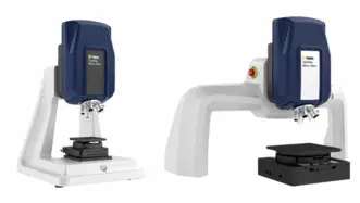
Micro-Profiler
Micro.View profiler systems are optimized for measurements with sub-nanometer resolution. With focused optics and high vertical resolution they enable detailed analysis of microstructures, surface finish and material distribution where even the smallest deviations matter.
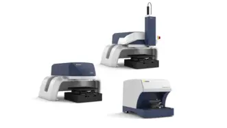
Macro Profiler
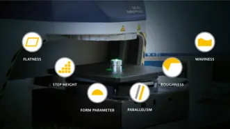
Pro.Surf inspects flatness, step height and parallelism on large parts and multi-part trays — non-contact, in seconds. No-crash telecentric optics measure even into bores, with the precision and repeatability production demands.
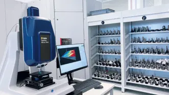
Roughness Deal Days
Save 30% on Polytec’s optical Roughness Tester—precise, non-contact 3D profilometry with sub-nm resolution. Offer valid until October 31, 2026.
Related applications and measurement tasks

Discuss your demands with our experts
Let’s start with a short discussion about your parts, tolerances, and workflow—and, if useful, we can add a feasibility study, PolyMeasure (contract measurements), or a PolyRent trial as optional next steps.