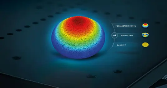
表面測定タスク
機能要件とプロセス要件は、地形と質感を定量化する標準化された表面パラメータを通じて表現される。以下のコレクションでは、各パラメータの詳細、評価のための推奨手法、および互換性のある測定システムについて説明する。
表面粗さ測定
表面粗さ測定の実践ガイド:適用されるパラメータと規格、よくある測定ミス、用途に最適な光学式プロファイロメーターの選び方を解説します。
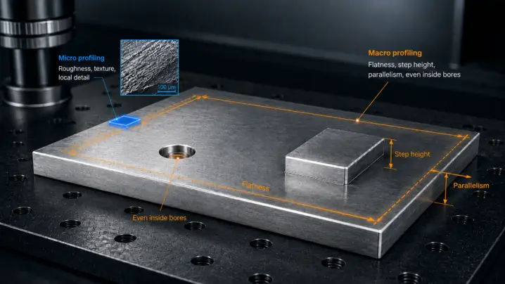
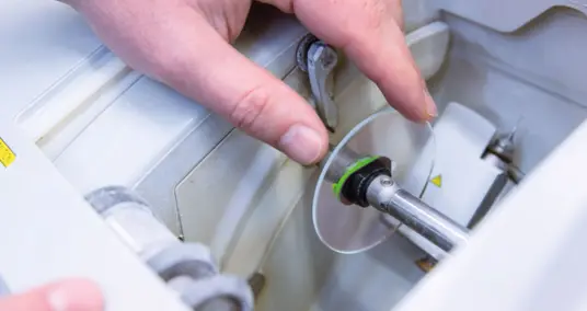
Maintain form and position tolerances
Verify form and position tolerances such as waviness, flatness, parallelism and tilt. Optical 3D surface metrology delivers reliable results—even in bores.
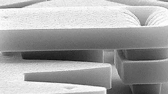
微細構造の表面計測
Topography & dynamics of microstructures and for nanotech. 3D geometry, roughness, and time-resolved motion.
平坦度、厚さ、平行度
Flatness, thickness and parallelism (FTP) measurement combines top & bottom topography measurement in a single shot.
コーティングと層厚
Coating quality control in 3D. Assessing pre-coat texture, post-coat defects, and film thickness.
トライボロジー解析
Tribology analysis with 3D surface profiler. Inspecting friction, wear and lubrication performance.
合格/不合格分析
WLIs deliver fast, objective and easy to use pass/fail feedback from areal 3D data. Sub-nanometer Z and recipe-driven workflows support inline SPC.
様々な産業における表面計測技術
異なる産業分野では、機能性、信頼性、および規格適合性に応じて、それぞれ固有の表面仕様が要求されます。以下のページでは、一般的な用途と部品、代表的なパラメータ目標値、および適切な計測手法とシステムについて概説します。
様々な作業領域における表面処理ソリューション
計測システムの要件は、環境や業務機能によって異なります。製造業ではスループットと使いやすさが重視され、大学・研究開発機関・品質管理ラボでは柔軟性と精度が求められます。
ポートフォリオ ― マクロからミクロの地形学まで
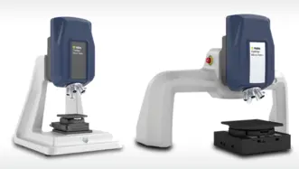
マイクロプロファイラー
Micro.View systems are optimized for ultra-high-resolution measurements in the sub-nanometer range. With focused optics and high vertical resolution they enable detailed analysis of microstructures, surface finish and material distribution where even the smallest deviations matter.
マクロプロファイラ
Pro.Surf は、大型部品やマルチパートトレイの平面度・段差・平行度を非接触でわずか数秒で検査します。衝突を防ぐテレセントリック光学系は穴の内部まで測定でき、生産現場が求める精度と再現性を実現します。
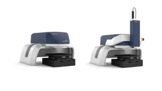
Metro.Lab
Metro.Lab is a compact, wide-area bench-top surface profiler. It combines high measurement performance with a small footprint — ideal for space- or budget-conscious applications that still require reliable 3D surface data.
どのプロファイラーが課題に適しているかお悩みですか? 2つのガイドが選択をサポートします。
2つの簡潔なガイドが重要な選択をご案内します。一方は適切な測定技術の選択を、もう一方は適切な測定スケール(ミクロかマクロか)の選択をサポートします。さらに、トライアル(試用購入)サービスをご利用いただけば、お客様自身の部品で選択を実際にご確認いただけます。
関連記事とストーリー
How CSI technology retrieves superior topography, form & roughness measurement data
Read how the optical technology of Coherence Scanning Interferometry (CSI) analyzes topography, form & roughness, where are sweet-spots, benefits and applications compared to related optical surface inspec…
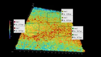
Characterizing surface texture, roughness, imperfections and scratches
Optical polishing is a fabrication technique developed specifically to achieve minimal defects and smooth micro-roughness values. Polishing is a process that involves the use of free grains, usually suspen…

Interview with Prof. Dr. Albert Weckenmann about optical and tactile surface measurement technology
We talked with Prof. Dr. Albert Weckenmann of the University of Erlangen-Nuremberg, Germany, about the limitations of tactile surface measurement technology and the opportunities of non-contact methods.
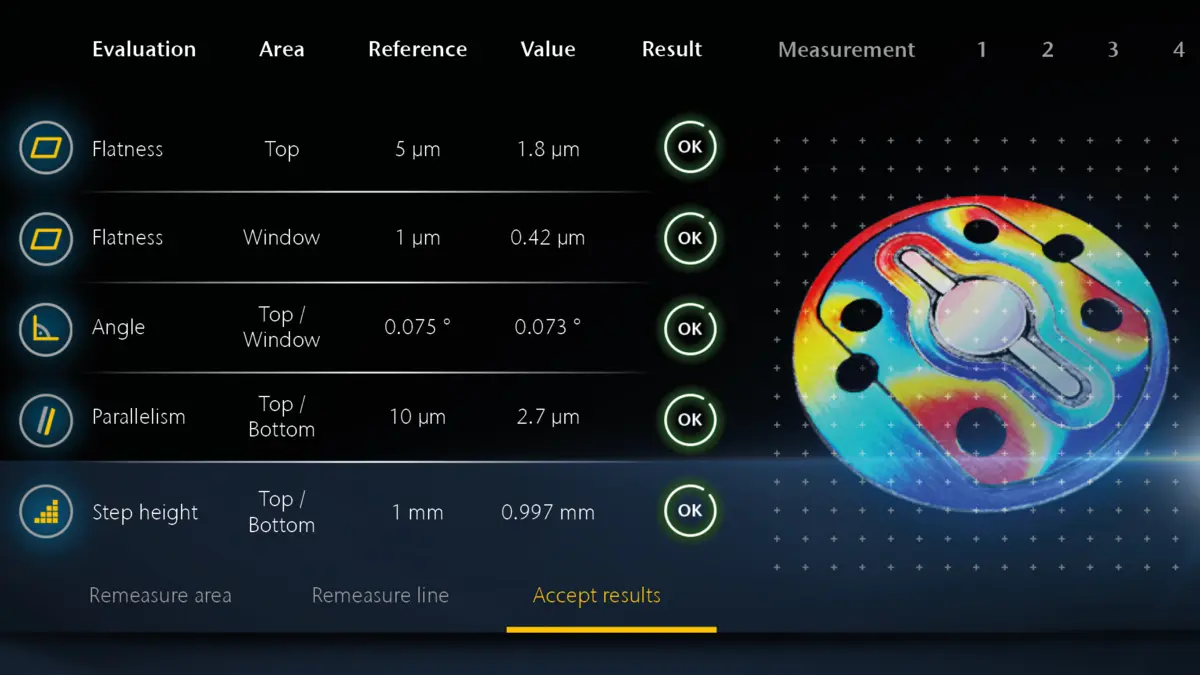
Confirm flatness, roughness and step height – TopMap quality control on the factory floor
Consistently producing high-quality precision parts is better achieved when the supporting metrology is tightly integrated with the manufacturing process. By combining Polytec’s TopMap optical metrology wi…
Overview of optical methods for surface metrology
For applications where tactile surface measurement techniques have shortcomings, non-contact optical instruments have been developed to overcome these shortcomings. Especially with the development of compu…

How surface metrology reveals the finest forensic details
Forensic science plays a vital role in the criminal justice system by providing scientifically based information through the analysis of physical evidence. During an investigation, evidence is collected at…