單次掃描捕捉高密度積體電路
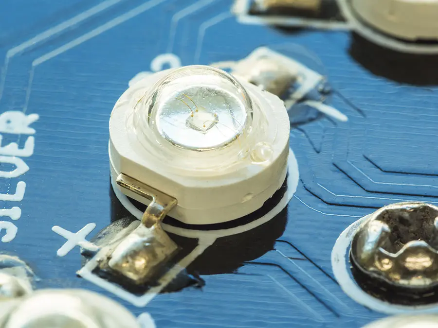
為確保高功率雷射二極體(HPLD)能穩定運作,必須驗證其封裝外殼具備正確的平面度與階梯高度規格。為達成此目標,應採用經實證技術,該技術能捕捉最微小的高度差異,並提供快速可靠的測量結果。此處所指的正是Polytec的表面測量系統。
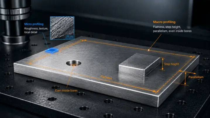
TopMap 光學3D表面測量系統能在大視野與大面積範圍內對雷射陣列中的二極體進行特性分析,直接在半導體表面解析「微笑曲率」與階梯高度。其大視野特性可於單次測量中捕捉所有細節,實現便捷、全面且高效的雷射二極體封裝檢測,同時維持高解析度表現。
用於二極體與電子元件的表面轮廓仪
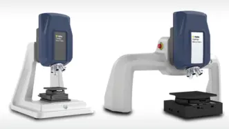
显微式形貌测量仪
Micro.View系列轮廓仪专为亚纳米级分辨率测量而优化。凭借聚焦光学系统与高垂直分辨率,可对微观结构、表面光洁度及材料分布进行精细分析——在最微小的偏差都可能影响性能的场景中,提供可靠的数据支撑。
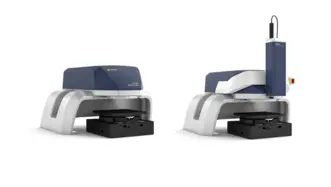
大视场3D轮廓仪
Polytec大视场3D轮廓仪Pro.Surf系列,专为生产环境设计。远心光学与真拼接技术实现大面积形状、平面度快速测量,可选配粗糙度测量功能。单次视场44×33mm,70mm Z轴范围,支持自动化。提供四年保修及先试后买服务。
Metro.Lab
Metro.Lab是一款紧凑型广域表面轮廓仪,将出色的测量性能与小巧的占地面积相结合,特别适用于空间或预算受限、但仍需可靠3D表面数据的应用场景。
选择合适的表面测量方案,可放心选用轮廓仪。通过我们的"先试后买"方案,让您轻松获益。
两份简明指南将带您完成关键决策:一份帮助您选择合适的测量技术,另一份帮助您选择合适的测量尺度——微观还是宏观。此外,通过我们的先试后买服务,您可以用自己的工件实际验证您的选择。