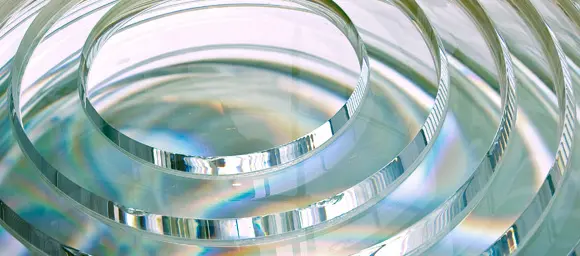
光學元件、玻璃及透明材料的表面形貌
透過精準測量形狀與粗糙度參數至(次)奈米級,確保透鏡、鏡片及光學元件等組件的品質與製造生產力。所有測量皆以高效能執行,以保障生產流程的產能輸出。
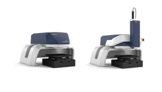
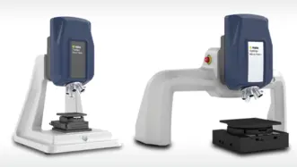
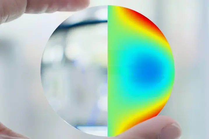
在TopMap 光學表面測量技術範圍內,為光學元件、玻璃或其他透明材料的品質檢測尋求高效測量與測試解決方案。Polytec的轮廓仪光學檢測系統具備靈活性與易用性,可快速實現奈米級精度的厚度測量,並判定形狀參數如平面度、階梯高度或平行度。
Polytec亦可根據粗糙度、距離或厚度需求提供客製化解決方案。您可受益於(次)奈米級解析度的精密數據,或運用大面積掃描技術一次涵蓋大型樣品甚至多組樣品。高速測量兼具高重複性:無論在生產線、製造環節或實驗室環境皆能適用。
- 測量透鏡與鏡片
- 設計自由曲面光學元件
- 檢測衍射光學元件 (DOE)
- 檢測雷射與光學設備等
測量透鏡、光學元件及鏡面的形狀、平整度與粗糙度
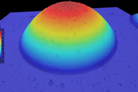
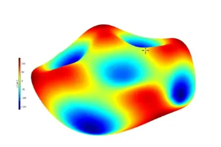
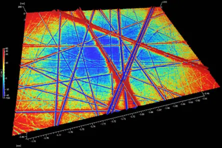
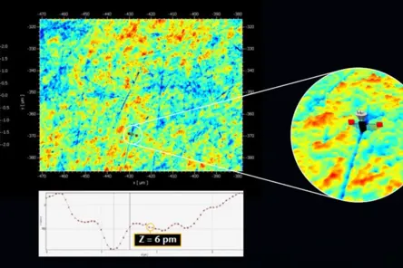
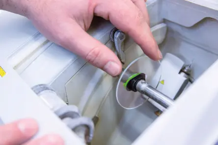
測量表面形狀參數,評估光學元件、玻璃及透明介質的平面度或台階高度。TopMap 表面轮廓仪技術可對透鏡、光學元件、自由曲面光學元件或鏡片進行完整且快速的檢測,以實現設計優化與製造品質控制。光學元件、鏡片或透鏡等透明材料因易受刮痕或缺陷(接觸式測量)及反射率(光學測量)影響,屬難測量材料。 採用非接觸式光學測量技術,可避免刮傷或觸覺測量探針的影響。Polytec的大面積地形掃描技術能一次捕捉整個工件或更大區域。其精密的SST智能掃描技術更能應對不同且具挑戰性的表面反射率,在啞光、霧面、鍍膜及亮面等表面均能提供可靠的測量性能。
典型光學檢測與量測任務
- 鏡面平整度測量
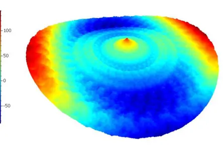
- 透鏡與自由曲面光學元件的完整三維特性分析
- 薄膜或層狀結構的彎曲度測量
- 層厚測量
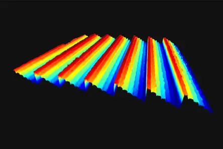
- 形狀、波紋與紋理的分離檢測
- 亞奈米級粗糙度與微結構分析
- 刮痕測試相關缺陷檢測與評估
- 精密機械部件(如鏡片或透鏡支架)的階梯高度測量
- 光學精密設備(雷射器、干涉儀等)之形狀公差檢測
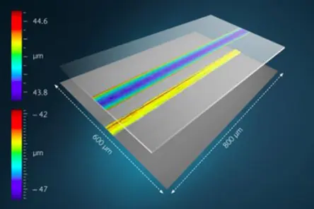
- 頂底面平面度-厚度-平行度一體化同步檢測

光學產業中的測量任務
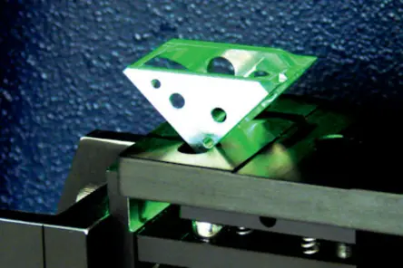
光學拋光
Superfinished surfaces and optical polishing demand non-contact, areal and high-precision white-light interferometers. Polytec profiler delivers remarkable results even with very reflective or transparent materials.
表面台阶高度
轮廓式台阶高度测量:基于面型数据,客观获取膜层/刻蚀深度及均匀性结果,支持符合ISO标准的报告输出与生产过程统计控制(SPC)。
膜层厚度
测量面型表面参数,精准控制膜层厚度,优化涂层工艺,助力降低质量成本。