Form and position tolerances in precision components
When manufacturing components, increasingly tight manufacturing tolerances must be met — particularly on technical and functional precision surfaces. Manufacturers therefore need to verify form tolerances such as waviness and flatness, as well as position tolerances such as parallelism and tilt, with high accuracy. This ensures compliance with specifications and reliable delivery within defined time frames.
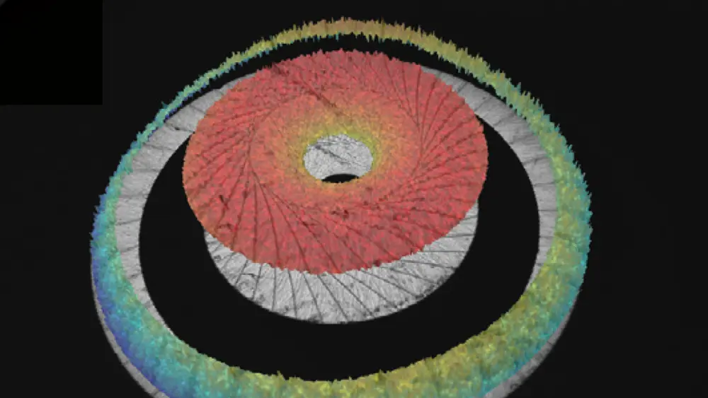
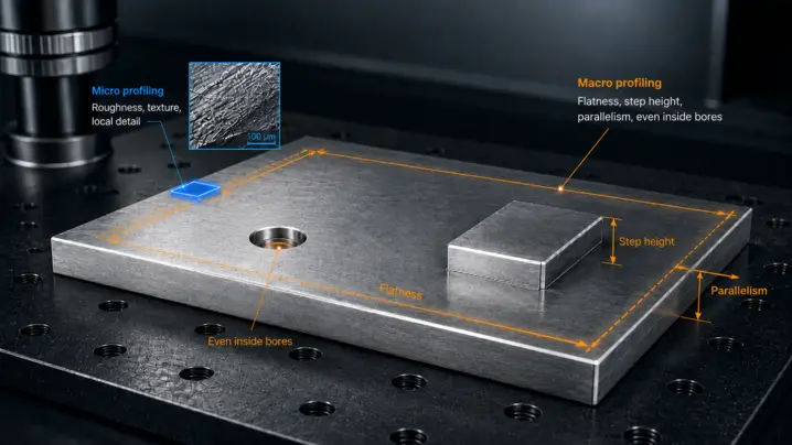
In many cases, manufacturers inspect the complete surface topography of a component to verify compliance with form and position tolerances — for example in shock absorber components, other precision components in the automotive and aerospace industries, or in fine mechanics.
Verifying form and position tolerances
White-light interferometry measures form parameters such as flatness, parallelism, and step-height faster and more efficient even for large samples. Working great on materials of different reflectivity, such as shiny polished metals or dull ceramics makes them the flexible choice for lab and production. Requirements for component warpage (e.g., printed circuit boards) also continue to increase as geometries shrink.
In addition, many applications involve challenging geometries: areas of interest may be located inside deep bores or show significant height differences between functional areas. Here, Polytec systems based on proven white-light interferometry deliver reliable results — where other optical measurement methods face limitations.
Polytec white-light interferometers perform repeatable, non-destructive measurements with resolutions down to a few nanometers — or even sub-nanometer capability. Optical profilers are ideally suited for the precise determination of form parameters such as flatness and parallelism — supporting efficient verification and easy integration into inline inspection workflows for form and position tolerances.
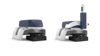
Optical profilers for tolerance verification
Polytec provides optical systems for measuring the topography of large surfaces with nanometer-level vertical resolution. This high vertical resolution is independent of the field of view, enabling stable measurement results across different sample sizes and inspection setups. Typical measurement tasks include determining flatness, step height, roughness, parallelism, and other surface parameters required to comply with form and position tolerances.
マイクロプロファイラー
Micro.View systems are optimized for ultra-high-resolution measurements in the sub-nanometer range. With focused optics and high vertical resolution they enable detailed analysis of microstructures, surface finish and material distribution where even the smallest deviations matter.
マクロプロファイラ
Pro.Surf は、大型部品やマルチパートトレイの平面度・段差・平行度を非接触でわずか数秒で検査します。衝突を防ぐテレセントリック光学系は穴の内部まで測定でき、生産現場が求める精度と再現性を実現します。
Metro.Lab
Metro.Lab is a compact, wide-area bench-top surface profiler. It combines high measurement performance with a small footprint — ideal for space- or budget-conscious applications that still require reliable 3D surface data.
どのプロファイラーが課題に適しているかお悩みですか? 2つのガイドが選択をサポートします。
2つの簡潔なガイドが重要な選択をご案内します。一方は適切な測定技術の選択を、もう一方は適切な測定スケール(ミクロかマクロか)の選択をサポートします。さらに、トライアル(試用購入)サービスをご利用いただけば、お客様自身の部品で選択を実際にご確認いただけます。
Related articles
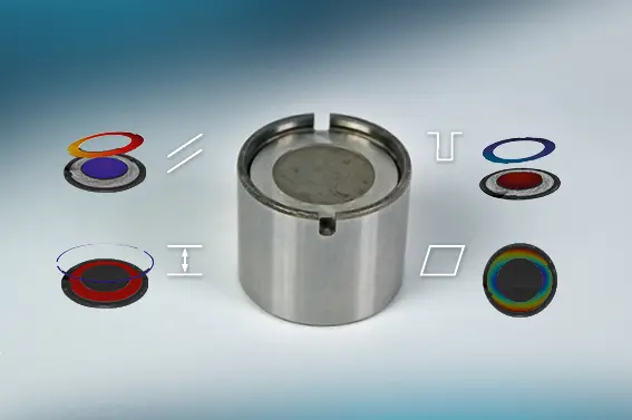
平坦度、厚さ、平行度
Flatness, thickness and parallelism (FTP) measurement combines top & bottom topography measurement in a single shot.
合格/不合格分析
WLIs deliver fast, objective and easy to use pass/fail feedback from areal 3D data. Sub-nanometer Z and recipe-driven workflows support inline SPC.
「購入前に試す」キャンペーン
Measure, rent, decide - on your terms. Make a confident decision about which surface profiler fits to your metrology strategy and safeguard your capital investment
ご要望について専門家とご相談ください
まずは部品仕様、公差、ワークフローについて簡単に話し合いましょう。必要に応じて、実現可能性調査、PolyMeasure(契約測定)、またはPolyRentトライアルをオプションの次のステップとして追加することも可能です。