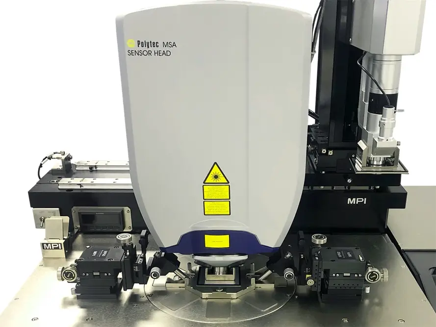
With the Micro System Analyzers (MSA-600, MSA-650 IRIS, MSA-100-3D), Polytec has for years been addressing the non-contact characterization of MEMS dynamics and topography from individual dies through to wafer-level measurements on probe stations. The latest enhancement combines this optical measurement technology with a certified cleanroom configuration and new automation functions that enable fully automated processing of complete wafer maps within externally managed laboratory and fab workflows.
New Technical Features for a Broader Range of Applications
- Cleanroom-Certified Configuration: MSA Micro System Analyzers are available in a configuration certified to cleanroom class ISO 3, making them suitable for demanding front-end processes.
- Automated Wafer Map Measurement: The goal is fully automated measurement and evaluation of all devices on a wafer, including resonance frequencies, quality factors, and mode shapes for each component.
- Script and Recipe Control: Within the Polytec PSV software, recipes can be defined for automated measurement sequences at the individual die level, which can then be scaled to full wafer maps via scripts and external controllers.
- Integration into Fab Workflows: Network-based remote control enables integration into fab-managed workflows, for example via a PLC of the production line.
- Setup time, including wafer alignment and script configuration, is typically only around 20 minutes for new devices or wafers.
- Automated grid alignment via image processing and autofocus ensure precisely reproducible measurement conditions and accurate results for every die across all wafers.
Application Context: Wafer-Level Testing of MEMS
The established approach for characterizing the dynamics of MEMS devices at wafer level uses a microscope-based scanning laser Doppler vibrometer system on a semi-automated probe station to non-contact capture resonances, mode shapes, and process variations. The automated sequence of coarse positioning, focus, contour detection, frequency sweep, and mode shape scan can now be implemented using the new MSA automation functions as a fully script- and recipe-based measurement cycle for every position on the wafer map.
Example of an Automated Workflow
- Transfer of a wafer map (coordinates/devices) from the fab database.
- Automatic XYZ positioning to the next die, autofocus, and grid alignment via image processing.
- Rapid single-point measurement for resonance detection, followed by a finely resolved frequency sweep and optional area scan of the mode shape.
- Feedback of measurement data for pass/fail classification to the fab-side MES/PLC system and statistical evaluation across the entire wafer.
Higher Productivity in MEMS Development and Manufacturing
- Higher Throughput: Fully automated measurement sequences reduce cycle time per die to seconds, enabling 100% testing in a production context.
- Early Removal of Defective Devices: Wafer-level testing prior to dicing sorts of out defective structures at an early stage, thereby reducing unit costs and scrap rates.
- Improved Model and Process Control: Denser datasets on resonance frequencies and mode shapes improve correlation with FEM models and enable monitoring of process drift (using dedicated test structures).
- Reliable Cleanroom Integration: The ISO 3-certified configuration of MSA systems simplifies qualification in regulated production environments and reduces the effort required for validation.
About the Micro System Analyzers
The Polytec Micro System Analyzers are optical measurement platforms for the static and dynamic 3D characterization of MEMS and microstructures from laboratory setups to integrated wafer-level measurement on probe stations. They combine laser Doppler vibrometry with high-resolution microscope optics and support frequencies from DC into the MHz and GHz range, including in-plane and out-of-plane vibrations as well as infrared transmission measurements for encapsulated structures.
Further information: