Surface metrology for quantum hardware—from qubit chip to cryostat
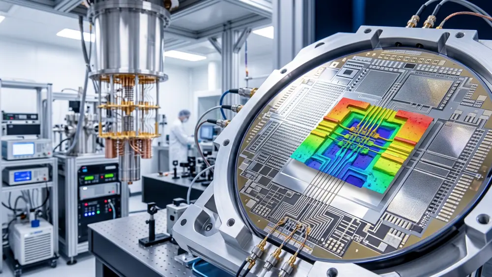
From the qubit chip to the cryostat, every stage puts different demands on surface quality. Here are the surface-critical challenges—what to measure at each, and which profiler handles it.

Flatness
- Capacitor pad
- Ion trap electrodes
- Wafer bonding
- Cold temp measurement
Form & step height
Qubit bonding
Planarity - electrodes, qubit
Package to chip
Bump compensable uniformity
Bond collapse
Chip gap uniformity
Wafer flatness & bow
Interposer flatness and gap
Roughness
Substrate roughness
Two-level system defects
Anomalous heating & roughness
Etch depths
放心选择适合您的表面轮廓仪,尽享“先试后买”服务
Challenges in quantum computing
and how surface metrology can help
Surface quality limits quantum hardware in different ways. For example parasitic two-level systems, scattering at etched sidewalls, bond-height variation, wafer bow and poor thermal contact. Expand each entry to see which parameters matter and how they are measured.
Surface losses on the qubit chip
In superconducting quantum processors, a large share of energy loss originates at material interfaces: the native oxides and microscopic defects at metal–air, metal–substrate and substrate–air boundaries act as parasitic two-level systems that drain qubit coherence.
In superconducting quantum processors, a large share of energy loss originates at material interfaces: the native oxides and microscopic defects at metal–air, metal–substrate and substrate–air boundaries act as parasitic two-level systems that drain qubit coherence. Surface roughness amplifies the problem—more effective surface area means more oxide, more defect sites, more loss. Ion traps face a related issue: motional heating of trapped ions scales strongly with electrode surface condition.
Areal roughness (Sa, Sq) of substrates and deposited superconducting films at sub-nanometer level; verification after etching, cleaning or passivation steps; roughness of trap electrode surfaces.
a micro profiler such as the TopMap Micro.View, which resolves sub-nm roughness without touching the delicate surface.
Structured features—trenches, waveguides, electrodes
Quantum devices are full of small, functional 3D structures: etched trenches in coplanar waveguide circuits, photonic waveguides where sidewall and surface roughness directly set scattering losses, microfabricated trap electrodes with critical edge and step geometries.
Quantum devices are full of small, functional 3D structures: etched trenches in coplanar waveguide circuits, photonic waveguides where sidewall and surface roughness directly set scattering losses, microfabricated trap electrodes with critical edge and step geometries. Here, the questions are dimensional: Is the etch depth on target? Is the step height uniform? Are edges clean?
Step height and etch depth verification, edge quality, local flatness of functional areas, roughness inside structured regions—ideally full-field, so uniformity across the structure is visible at a glance.
TopMap Micro.View—areal measurement captures the whole structure in one dataset, which can be re-analyzed later without re-measuring the part.
3D integration—bump bonds and chip stacking
Scaling beyond a few hundred qubits pushes processor architectures into the third dimension: qubit chips are flip-chip bonded to wiring or interposer chips via indium bump arrays, with chip-to-chip gaps of only a few micrometers.
Scaling beyond a few hundred qubits pushes processor architectures into the third dimension: qubit chips are flip-chip bonded to wiring or interposer chips via indium bump arrays, with chip-to-chip gaps of only a few micrometers. Gap variation across the die shifts qubit frequencies and coupling strengths—so bump height uniformity and chip flatness before bonding decide device yield.
Bump coplanarity across the full array, chip bow and warp, flatness of bonding areas, parallelism verification.
TopMap Micro.View with the additional 0.6x wide-field objective—extending the field of view to capture full bump arrays and small dies in a single measurement.
Form and flatness at chip and wafer level
Underneath the nanoscale physics sits a classic precision-engineering task: substrates, carriers and interposers must be flat.
Underneath the nanoscale physics sits a classic precision-engineering task: substrates, carriers and interposers must be flat. Wafer bow, total thickness variation and warp propagate into every subsequent process step—from lithography focus to bonding gaps.
Flatness, waviness, bow and TTV over large areas; parallelism of mating parts; form deviation of machined carriers and packages.
a macro profiler such as the TopMap Pro.Surf—its telecentric optics measure large areas with uniform accuracy across the full field.
The cryogenic periphery
Often overlooked: quantum processors operate inside dilution refrigerators at millikelvin temperatures, where thermal contact between mating surfaces is everything.
Often overlooked: quantum processors operate inside dilution refrigerators at millikelvin temperatures, where thermal contact between mating surfaces is everything. Thermal boundary resistance depends directly on the flatness and roughness of cold-stage interfaces, and vacuum integrity depends on sealing surface quality. A leaking flange or a poorly seated thermal joint costs days of cooldown time.
Flatness and roughness of thermal contact surfaces, sealing and flange faces, machined cryostat components—typically larger metal parts where fast, full-field inspection beats tactile spot checks.
TopMap Pro.Surf, designed for exactly this class of functional surfaces on machined parts.
Why Pro.Surf is the perfect match for quantum R&D and inline quality control
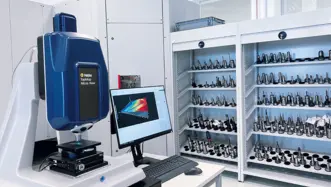
Pro.Surf optical profiler
//Pro.Surf is designed for quality engineers, production managers and metrology teams who need reliable pass/fail decisions on complex components in industrial environments. Where conventional profilometers struggle with bores, recessed features or large part trays, Pro.Surf uses telecentric optics and a large field of view to maintain measurement accuracy across the full area.
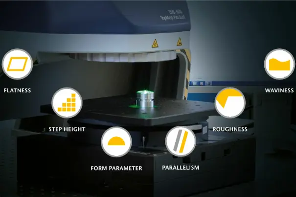
- Seamless measurement through cryostat windows
- Non-contact optical measurement enables access to critical surfaces through optical viewports—without disturbing sensitive quantum hardware.
- Single-FOV measurement of the entire device
- Capture large functional areas or complete devices in a single field of view, minimizing stitching and improving measurement efficiency.
- Unparalleled automation capabilities
- From automated positioning and measurement routines to repeatable evaluation workflows, Pro.Surf is built to support both advanced R&D and inline quality control.
- Uncompromising data quality for the highest accuracy demands
- Generate highly repeatable, reliable 3D measurement data where precision and confidence in every result matter.
- A system architecture that adapts to your needs
- Configure the measurement setup around your device, process and workflow—not the other way around—providing flexibility from laboratory development to scalable production.
From macro to micro profiler for your quantum computing requirements
Quantum devices are fragile, expensive and often one-of-a-kind. Non-contact optical profiling measures without any risk of scratching a film or deforming a bump—and because every measurement captures a complete areal dataset, results can be re-analyzed with new parameters at any time, without access to the original part. For teams moving from research into small-series production, that combination of speed, gentleness and traceability is usually the deciding factor.
Not sure which configuration fits your parts? The most reliable answer comes from measuring your own samples—talk to us about a demo measurement or a rental system to test under real conditions.
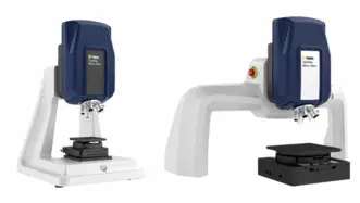
三维光学轮廓仪
Micro.View 系列三维光学轮廓仪专为亚纳米级分辨率测量而优化。凭借聚焦光学系统与高垂直分辨率,可对微观结构、表面光洁度及材料分布进行精细分析——在最微小的偏差都可能影响性能的场景中,提供可靠的数据支撑。
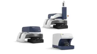
大视场三维光学轮廓仪
Pro.Surf 可对大型工件及多样本料盘进行平面度、台阶高度与平行度检测——非接触、数秒完成。防碰撞远心光学系统可深入深孔内部进行测量,满足生产环节对精度与重复性的严苛要求。
Roughness Deal Days
Polytec光学Roughness Tester限时优惠30%:精准的非接触式3D轮廓测量,分辨率达亚纳米级。优惠截至2026年10月31日。