微结构测量与微技术测试
在消费电子、汽车、可穿戴设备以及医疗科技等领域,功能组件的小型化催生了大量的应用与创新。微机电系统(MEMS)和微光学技术对精密测试有着极高的要求,给相应的测量技术和测试工具带来了新的挑战。复杂的微结构需要进行全面的分析,最为理想的是开展高分辨率( μm ~ nm 级别)的面扫描检测,从而深入了解其质量与功能方面的特性。
Polytec 的光学测量解决方案,不仅能够对表面的形貌、形状以及结构细节进行表征,还可以对微机电系统和微系统的动态运动情况以及性能表现进行测试 。
微结构静态形貌测量
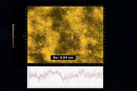
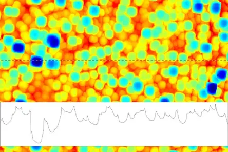
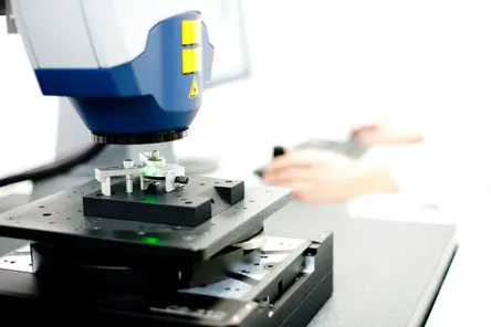
微结构及微机电系统 MEMS,需严格契合公差标准,才能保障功能稳定与使用期限,同时要避免微观结构遭受物理损伤。因此,非接触式光学表面特性分析,是无损检测微技术、评估表面形状与粗糙度等参数的关键。Polytec 光学计量解决方案,可对微结构和微系统开展无干扰、可重复测量。
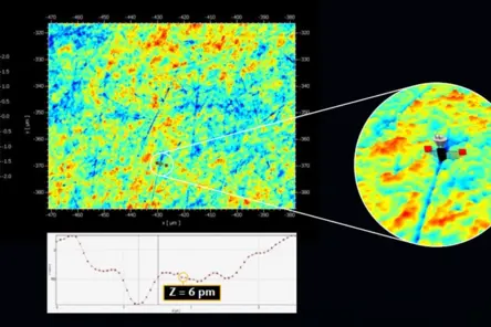
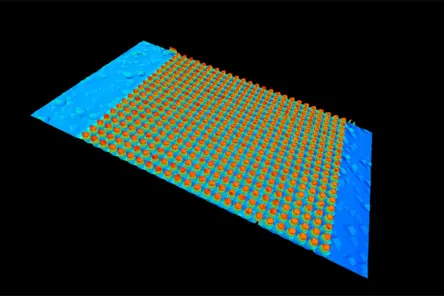
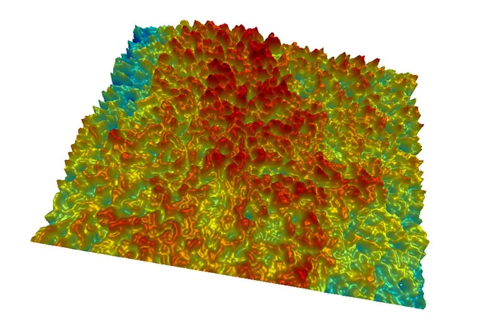
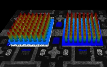
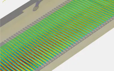
TopMap 3D 表面测量基于相干扫描干涉技术,能扫描高度数据,数秒内采集数百万个表面测量数据,不受材料限制,无论是数控加工后的粗糙材质,还是晶圆类光滑反光材料,都能精准测量。其智能表面扫描技术,可轻松测量样本的不同反射区域。
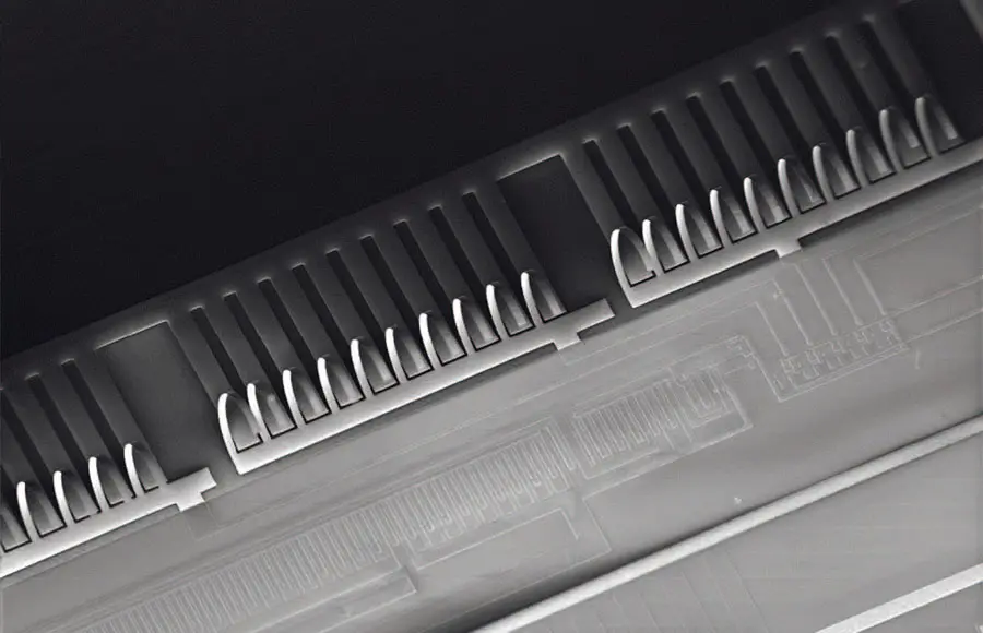
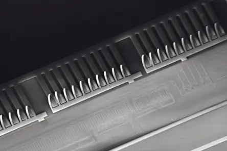
微结构静态形貌测量广泛应用于微传感器、微执行器检测,金属纹理板、密封表面或机加工表面研究 —— 这些场景都需确保良好润滑。此外,在化妆品、医疗技术领域的生物医学样本研发中,该技术也发挥着重要作用。
Downloads
MEMS 动态测量
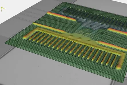
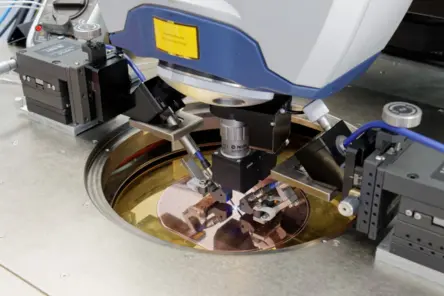
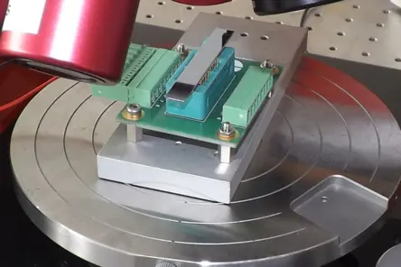
主动式微机电元件(如 MEMS 执行器和传感器)仅靠电气表征不够,需先进光学测量技术。Polytec的MSA 显微式激光测振仪,可全面表征微系统动态特性。该 MEMS 测试系统能精准评估高分辨率表面形貌和元件动态特性。
测量技术
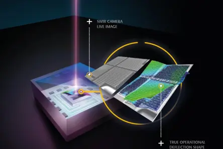
其动态特性测量运用激光多普勒测振技术,可进行 GHz 宽带测量,高分辨率呈现元件模态振型和真实相位,常用于模型验证。专利 IRIS 技术可透过硅封装检测 MEMS 动态,实现成品测试。

微结构的接触式与光学测量方法对比
接触式表面测量技术在微结构分析上存在局限性。借助二维轮廓线,难以获取整个表面的复杂结构细节,且测量耗时久。这类测量常以粗糙度轮廓线为参考,开展后续评估。此外,触针测量会在表面留痕、造成自身磨损,影响测量重复性。
非接触式光学检测技术,在机械工程精密表面检测中优势突出。它测量可重复,不会产生废品,在全表面测量和 100% 抽检场景下,效率更高、成本更低。
我们可为您测量样品,并通过免费可行性研究,展示实际成效!
相关产品
Micro.View
TopMap Micro.View® is an easy to use optical profiler in a compact table-top setup. Choose Micro.View® as the cost-effective inspection tool for examining precision-engineered surfaces down to the sub-nm range, for inspecting roughness, microstructures and more surface details.
Micro.View+
Advanced microscope-based surface profiler with automation and color imaging. Micro.View+ enables repeatable, operator-independent roughness and texture analysis—ready for lab and production use.
MSA-600 显微式激光测振仪
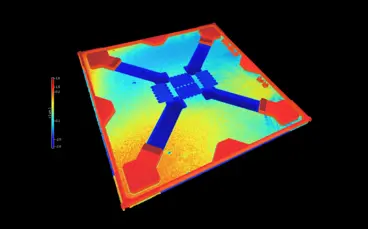
MSA-600 显微式激光测振仪专为 MEMS 及显微结构测量而打造,是一款能够获取三维静态与动态特性的一体化光学测量解决方案。它在加速产品开发流程、优化产品质量控制方面表现卓越,甚至可集成至商用探针台,用于晶圆级测试。目前,该仪器的性能已提升至高达 8 GHz。
MSA-650 IRIS 显微式激光测振仪
Polytec全新的最先进的且已获得专利技术的MSA-650 IRIS显微式激光测振仪,是目前世界上唯一能透过硅封装结构(无需拆除硅帽)获取硅器件面内和面外动态特性的系统,测试带宽覆盖DC~25 MHz。
MSA-100-3D 显微式激光测振仪
3D显微式激光测振仪同时记录XYZ三个方向的振动分量,测试带宽覆盖DC~25 MHz,每向的振幅分辨率均达到亚皮米级,可用于面内和面外振动测试。
MSA-060显微式激光测振仪
MSA-060显微式激光测振仪是一款紧凑型光学测量系统,用于全面评估MEMS和微系统的振动特性、精密机械动力学和电子产品的可靠性,测试带宽覆盖DC~24MHz。 系统采用激光作为探测手段,以非接触、无损检测方式帮助用户获取被测微型元器件的动力学特性。


与Polytec专家进行交流
Our experts are ready to support your projects with tailored measurement solutions or support you in measuring what matters — get in touch with us today.