Fast and precise aerial measurement of layer thickness
The PVA Vision systems use a unique combination of optical spectroscopy and imaging for precise surface analysis. Depending on the material properties, layer thicknesses can be measured non-destructively in an impressive range from 1 nm to 500 µm.
The technology enables inspection on a wide variety of substrates such as semiconductors (Si, SiC), metals, glass, and polymers. In a single measurement run, the layer thickness is spatially resolved across the entire sample area. Deviations from production specifications as well as defects or contamination are reliably identified.
“ The focus was on a straightforward, honest design. It focuses on the essentials and thus makes this complex technology accessible.”
Non-destructive and non-contact inspection of ultra-thin layers
Layer thicknesses can be measured non-destructively in a range from 1 nm to 500 µm on a wide variety of substrates such as semiconductors, metals, or glass. At the same time, the system reliably detects defects, contamination, or deviations from production specifications.
Fast measurement and evaluation
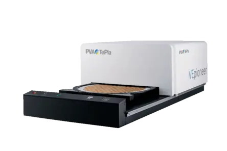
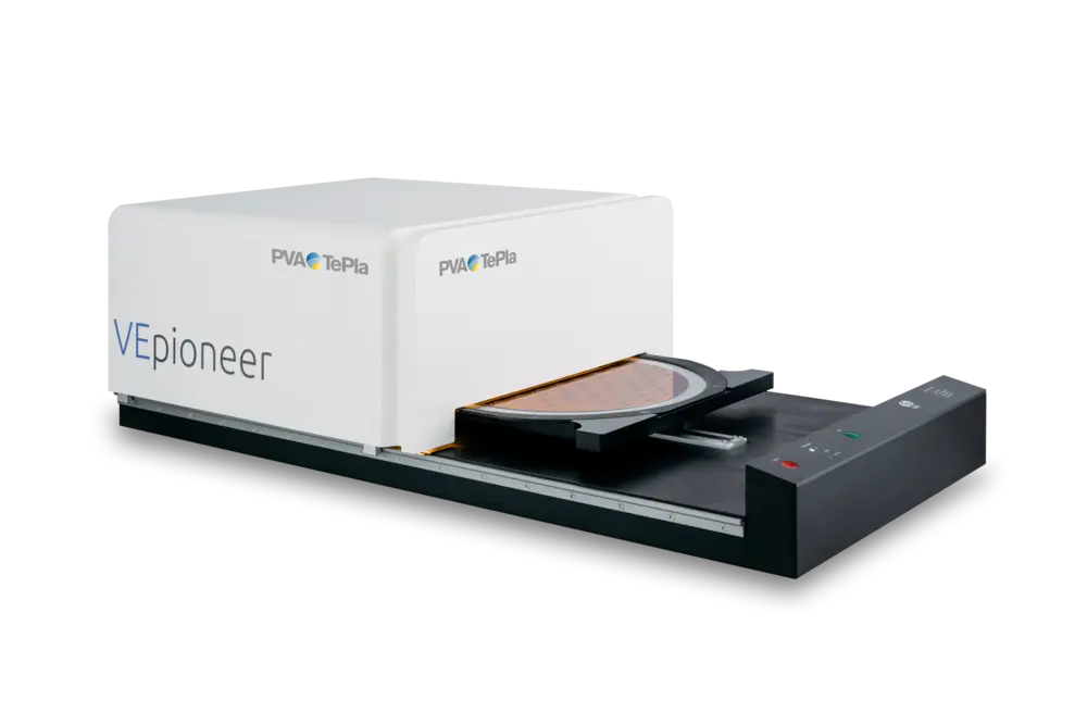
Bench-top systems typically require less than 20 seconds for a comprehensive analysis.
Complete sample information in a single pass
The systems combine optical spectroscopy with imaging analysis to capture 100% of the sample information in a single measurement run. This technology enables spatially resolved detection of chemical, electrical, and optical properties.
Flexible hardware and software customization
The systems can be precisely configured using different light sources and wavelength ranges of the sensors (VNIR, SWIR, NIR) as well as customer-specific sample recordings. Evaluation is carried out efficiently using the specialized VEsolve PRO software on standard computers.
Features
//- Contactless and non-destructive measurement
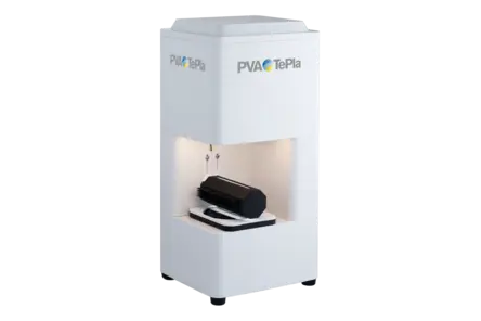
- Compact bench-top systems
- VEpioneer Core: to be announced
VEpioneer Macro: 1002 x 530 x 331 mm - Measurable layer thicknesses
- 1 nm to 500 um (depending on material)
- Measurement time for entire sample
- less than 10 s (typical)
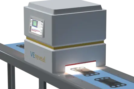
Inline modules: Frame rates below 4 ms possible - Sample mounting
- typical wafer sizes or customized
- Powerful software