表面特性評価によるエポキシダイボンディングの制御
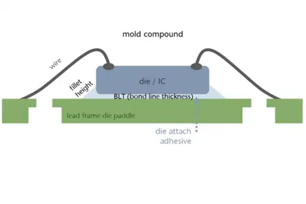
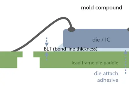
エポキシダイボンディングおよび関連するダイアタッチプロセスでは、わずかな偏差でもプロセスの安定性、部品の信頼性、寿命に影響を及ぼす可能性があります。そのため、ボンディングライン厚さ(BLT)、ダイの傾き、位置決め精度といった主要な品質指標を、信頼性高く再現性をもって監視する必要があります。
Polytec TopMap 光学式表面プロファイラーは、エポキシダイボンディング工程の高速非接触検査を実現します。ダイの向きや傾斜からボンディングライン厚さに至るまで、生産環境下で直接、自動化された品質管理のための精密な3D表面データを提供します。
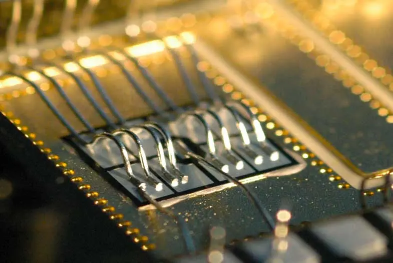
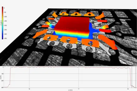
QFNパッケージ(クワッドフラットノーリード)の特性評価
TopMap 3D表面計測ソリューションは生産ラインに容易に統合され、エポキシダイボンディング工程において自動化された高解像度の工程内測定を実現します。代表的な検査タスクには以下が含まれます:
- ダイの傾斜と位置決め
- ボンディングライン厚さ(BLT)およびBLT高さ
- 基準特徴に対するねじれ角と相対位置決め
QFNパッケージにおいて、ダイエッジに沿って隆起する接着剤の余剰部分であるダイアタッチフィレットは、機械的安定性に重要な役割を果たします。精密なBLT測定に基づき、フィレット幅、高さ、傾斜角などの関連パラメータを評価・最適化することで、プロセスの堅牢性と部品品質を向上させることが可能です。
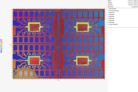
接着剤の線幅、フィルムおよび層の厚さの3D測定
表面形状測定装置
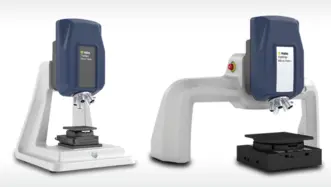
マイクロプロファイラー
Micro.View systems are optimized for ultra-high-resolution measurements in the sub-nanometer range. With focused optics and high vertical resolution they enable detailed analysis of microstructures, surface finish and material distribution where even the smallest deviations matter.
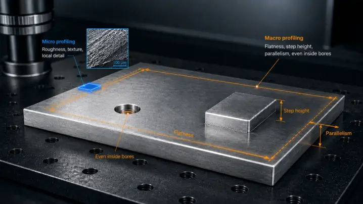
マクロプロファイラ
Pro.Surf は、大型部品やマルチパートトレイの平面度・段差・平行度を非接触でわずか数秒で検査します。衝突を防ぐテレセントリック光学系は穴の内部まで測定でき、生産現場が求める精度と再現性を実現します。
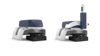
Metro.Lab
Metro.Lab is a compact, wide-area bench-top surface profiler. It combines high measurement performance with a small footprint — ideal for space- or budget-conscious applications that still require reliable 3D surface data.
どのプロファイラーが課題に適しているかお悩みですか? 2つのガイドが選択をサポートします。
2つの簡潔なガイドが重要な選択をご案内します。一方は適切な測定技術の選択を、もう一方は適切な測定スケール(ミクロかマクロか)の選択をサポートします。さらに、トライアル(試用購入)サービスをご利用いただけば、お客様自身の部品で選択を実際にご確認いただけます。