
Measure and map sheet resistances
A layer’s sheet resistance and information derived from the same – such as the specific resistance, the charge carrier density or the layer thickness – are basic parameters that are needed in many fields of the semiconductor and photovoltaics industries. The four-point measurement technique is a proven method for determining these parameters.
4Dimensions’ more than 35 years of experience in this field is reflected in the sheer diversity and many sophisticated detailed solutions of the systems presented here.
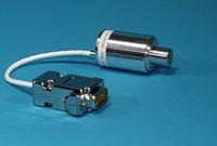
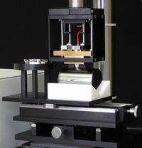
Scan Heads
The measuring stations can use cylindrical scan heads with a wide range of different tip arrangements and geometries. We have defined a series of standard scan heads to make the selection process easier.
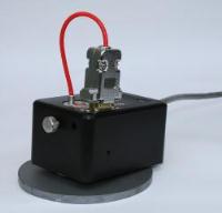
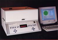
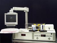
Simple Hand-Held and Laboratory Devices
Polytec’s product range includes simple and affordable measuring stations for conducting manual measurements or even a variety of manual tables. Simple measurement electronics automatically adjust the power and show you the result as both a current and voltage value and as sheet resistance.
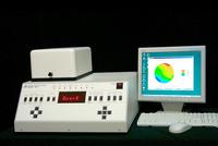
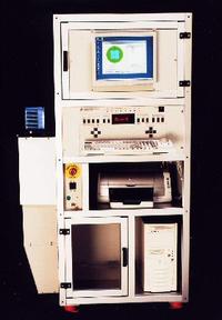
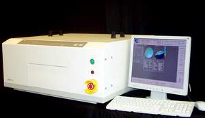
Mapping 4PP for 6” Solar Cells or 8” Semiconductor Wafers
The desktop devices in the 280 series are widely used. Computer-controlled and featuring a motorized table, you can use them to measure the layer resistance distribution on wafers measuring up to 200 mm in diameter or on solar cells up to 156 x 156 mm and then illustrate the results in contour and 3D graphs (wafer maps).
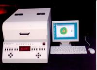
Mapping 4PP for 8” Solar Cells or 12” Semiconductor Wafers
These models are suitable for wafers up to 300 mm in diameter or solar cells measuring up to 210 x 210 mm.
Photovoltaic Extensions
In addition to the classic task of determining the layer resistance, the modified 4PP measures the leakage current of the P/N junction or the metallization’s contact resistance.
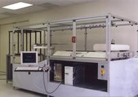
Fully Automatic “Cassette to Cassette” Systems for Production
The “cassette to cassette” systems for 200 and 300 mm wafers are fully automatic systems for production. They save space in clean rooms thanks to a sophisticated handling concept. Automatic switching between several scan heads, automatic wafer alignment or a FOUP variant for 300 mm wafers are available as options.
Ingots
Polytec adjusts the measuring technology to your crystal’s dimensions. Manual measuring stations with a hand-operated scan head lowering fixture, for instance, have already been implemented, as have automatic measuring systems that record the resistance value and the temperature along the crystal and illustrate the adjusted results in a 2D plot.
III-V Semiconductor
A dynamic alternating current overlay method solves contact problems caused by the Schottky diodes that form on the junctions of metal semiconductors.
Mercury Contact
This system uses mercury as the contact material instead of needles. Since virtually no contact force is exerted on the contacted surface, the four-point measurement can also be carried out on extremely thin layers.
Flat Panel and Special Sizes
This series includes four-point measuring systems with adapted dimensions for an extremely wide variety of flat panel display applications.