as 3D profile")
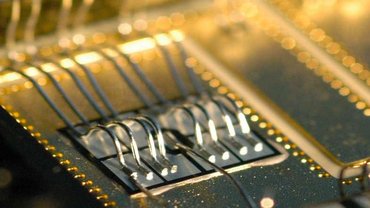
Optical inspection of PCB and BGA
The reliability of PCB and the respective PCB components like IC (integrated circuit) or BGA (ball grid array) can vary with every design and selection of semiconductor components installed. For each type and series of PCB design, ideally automated, in-process quality control and testing of PCB is needed at manufacturing. In addition, at customer level for inspecting for “dead on arrival” issues, caused for example by breaking on weak points during transportation, quality control methods are part of the process. TopMap optical 3D surface metrology allow fast scanning of entire sample surfaces with nanometer resolution, providing areal topography data of PCB, IC and BGA in a single shot.


 bump areal measurement with large field of view")
 bump measurement in 3D")
Types of ball grid array packaging
Looking onto the history of semicon packaging, there were DIPs (dual in line package) at first, QFP (quad flat package) or QFN (quad flat no leads), BGA (ball grid arrays) as one of the most popular packaging techniques, leading to the always higher pin count. BGA are well established in consumer electronics such as smartphones, tablets, motherboards and digital cameras. In comparison to DIPs and QFPs: the BGA shows more I/O connections, shorter connectors leading to improved performance and high speed. Bump materials typically are SnPb , SnAgCu , SnIn, SnBi with bump diameters typically reaching 90-400 µm and a distance between bumps of around 0.1 to 2 mm.


Typical failure and defects in BGA manufacturing
In the manufacturing of BGAs, for example using the flip chip method, which describes the connection by applying heat and pressure on the substrate, typical manufacturing errors or defects can occur when the pitch is too high or the bump is too small or too big. Polytec TopMap surface profilers are ideal metrology solutions for areal measurement and inspection of ball height / bump height, coplanarity, chip flatness and chip warpage, bga ball flatness, for optical inspection of the entire BGA pitch or focusing on the shape of the pure ball tip in an optical and non-contact way.
How do you control BGA quality?
What parameters do you measure on ball grid arrays?
BGA warpage & quality control


Another BGA manufacturing issue is the uncontrolled warpage – a phenomena of areal deformation of the entire surface of a PCB or a BGA, causing unconnected areas and defects on the BGA. If the warpage is not under control, even the perfectly manufactured ball grids would not fullfill the desired functional behavior, leading to the BGA improperly fitting into the board. Optical profilers like TopMap white-light interferometers reliably detect warpage on large areas in a non-contact way in 3D – allowing clear damage detection as valuable feedback for the BGA manufacturing process.
3D profiling as quality inspection of ball grid arrays
Using 3D optical profilers for areal and non-contact characterization can be powerful quality control tools: For measuring topography of electronic components, testing of printed circuit boards (pcb testing), solder bumps, ball grid array flatness measurement, pass-fail analysis and process trouble-shooting in the manufacturing of PCB. Providing valuable feedback for the production process of PCB and electronics, optical profiling can be an efficient integral part of the quality control process of electronics and micro-electronics. Usually, more advanced and complex PCB are applied and designed layer by layer which might require layer thickness measurement and distinguishing several layers. Here, optical testing solutions from Polytec open up a realm of solutions for measuring layer thickness as one quality indicator.
For characterizing PCBs for failure analysis, checking BGA flatness in a non-contact way, for free feasibility studies and a first sample report, contact us.
Related products

TopMap Pro.Surf
Pro.Surf stands for fast and professional 3D surface characterization: Capturing 2 million measurement points within seconds make sure to see every detail. Pro.Surf masters challenging production workflows with short measuring times. The exceptionally large field-of-view (FOV) 44x33 mm captures big samples or even multiple samples in a single shot - while stiching expands to 230x220 mm with the large 70 mm Z range for enhanced flexibility.

TopMap Micro.View
TopMap Micro.View® is an easy to use optical profiler in a compact table-top setup. Choose Micro.View® as the cost-effective inspection tool for examining precision-engineered surfaces down to the sub-nm range, for inspecting roughness, microstructures and more surface details. Custom objectives 0.6x to 111x and stage options allow for application-specific finetuning.

TopMap Micro.View+
TopMap Micro.View®+ is the next generation optical surface profiler in a modular design to measure challenging workpiece textures, surface finish and microstructures or MEMS with sub-nm resolution. Focus Finder and Focus Tracker assist in keeping samples focused at all times along the exceptionally large 100 mm Z range, with fully motorized positioning ready for both labs and automation. Challenge it now!
Further applications
- Die bonding
![Elektrisch leitendes Kleben in der Elektronik]()
- Flexible electronics

Surface analysis and and quality control on flexible electronics and printed electronics - High power laser diodes

Inspection of flatness and step-height on high power LED - Mobile devices

Production testing of components for mobile devices using 3D optical surface metrology - Pass/fail analysis

Large image field and automatic pattern recognition allow multi-sample measurements in one shot - without manual positioning or fixture - Surface parameters

Surface parameter characterizing the form, waviness and texture of a workpiece