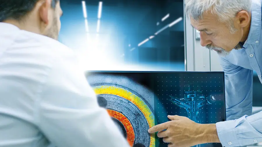
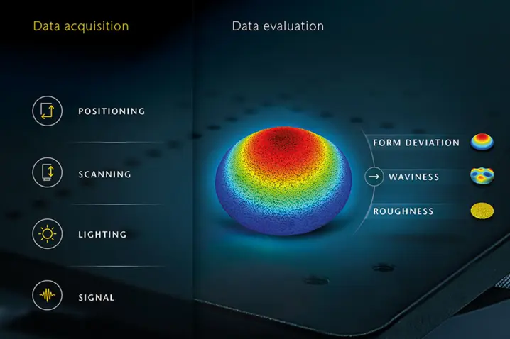
Why Polytec optical profilometers fit your surface metrology application
Our portfolio covers optical profilometers for a wide range of metrology tasks—from microscope-based systems for microstructures to macro and bench-top optical profilers for large-area form and quality inspection.Largest XYZ area sampling thanks to the broadest single-shot FoV and full usable Z-range.
- True Stitching extends measurement field to ~230 × 220 mm while achieving the highest accuracy
- Outstanding measurement precision reveals surface details down to 0.01 nm Z-resolution.
- Any-surface measurement with SST Smart Scanning Technology.
- Easy operation and automation-ready features & interfaces.
- Modular concept enables custom configurations and upgrades, expanding your capabilities.
- Long-term reliability due to rugged design and a 4-year warranty.
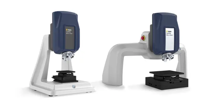
Micro.View+
Highest repeatability and reproducibility in sub-nm resolved inspection of texture, roughness, finish and structural details with automated workflows.
Micro.View
Our easy to use, table-top optical profiler. Texture, roughness and microstructure analysis as an affordable yet modular package.
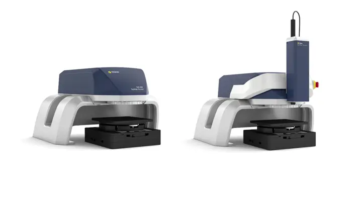
Metro.Lab
Complete and compact test bench for large area form characterization - even with a smaller budget! For QA labs and case-by-case quality inspections in manufacturing.
Pro.Surf+
Multi-sensor profiler for fast large area topography scanning, repeatable measurements and combined form & roughness characterization resolved in the nm range.
Pro.Surf
For fast, large-area topography, form and flatness measurement. Telecentric optics with large Z range reaches holes, largest FoV and true stitching accuracy allow efficient multi-sample measurements.
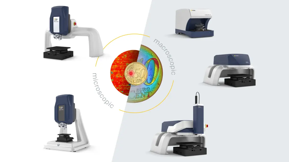
Differences between optical profilometers: micro and macro systems
The TopMap portfolio is structured into three CSI optical profiler lines Micro/ Macro/ and Bench/ — each optimized for certain sample sizes, resolutions, measurement tasks, and throughput needs.
- Micro profilers: High lateral resolution for roughness, texture and microstructures.
- Macro profilers: Large-area form measurement with telecentric optics, fast and repeatable for high throughput.
- Bench profilers: Compact, cost-effective wide-area measurements for labs and quality control.
The table below provides a rough overview about the main differences between our micro, macro, and bench profilers. Use it to identify the family that best matches your required field of view, precision, sample size, and throughput. And feel free to use our "try before buy" offer to safeguard the best possible investment decision.
| Profiler type | Field of view | Strengths | Measurement tasks | Best suited for |
| Micro Profiler | From 0.07 up to 3.7 mm | Highest lateral resolution, sub-nm vertical accuracy. | Surface texture, roughness analysis, focused tribology | MEMS, micro-optics, microfluidics, precision parts. |
| Macro Profiler | Single FoV 44 × 33 mm, with True Stitching up to 230 × 220 mm and more | Large-area form measurement, telecentric optics, stable geometry. | Flatness, parallelism, step height, thickness, form measurement deviation. Roughness with Pro.Surf+ | Quality inspection in precision manufacturing, small to large parts and trays. |
| Bench Profiler | 37 × 28 mm | Compact, cost-effective wide-area metrology. | Form deviation, step height, case-by-case quality inspection. | Sample inspection in manufacturing. |
Our 3D optical profilometers in depth—from micro to macro.
Below you’ll find descriptions of each CSI optical profilometer type to help you compare capabilities and select the right system for your measurement task. In case you are not sure what fits best to your metrology strategy, use the contact form at the end to talk to our experts.
TopMap micro profiler
Microscopic, high-resolution 3D optical profiler for surface topography measurement with high lateral resolution—best for analysis of microstructures, precision components and optics, MEMS, and high precision tribology.
- Variable FoV with spot sizes from 0.07 to 3.7 mm.
- Ideal for sub-nm resolution.
- True Stitching enables highest precision on wider areas.
Choose Micro.View white-light interferometers when maximum lateral resolution and high repeatability is key for your microstructure analysis and ultra-precision machined surfaces.
Macro profiler - Pro.Surf and Metro.Lab
Super efficient macro surface profilometer best for large-area surface form measurement and trays. Pro.Surf is the preferred profiler in manufacturing due to the reliability, efficiency and flexibility.
- Captures up to 2M data points within just seconds
- Outstanding single FoV up to 44 × 33 mm—expandable to 230 × 220 mm with True Stitching.
- Measures flatness, shape, parallelism faster—even inside bores.
- Pro.Surf+ adds a chromatic confocal sensor for combined 2D roughness examination.
- Ideal for precision mechanics, sealing surfaces, watchmaking, and optics
Choose Pro.Surf when you need large-area, high-throughput form deviation measurement with maximum stability.
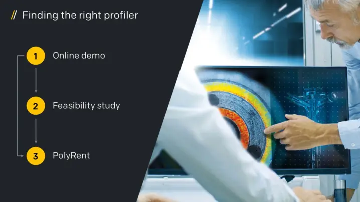
Choose the right surface profiler with confidence—benefit from our "try before buy" approach.

Turn profilometer operation into standardized, repeatable workflows.
Get the most from your 3D optical profiler: accelerate quick quality checks, support in-depth research, and enable your team to measure with confidence.
- Intuitive 2D & 3D visualization
- Recipe-based workflows (SOPs)
- Full automation readiness (MES/PLC)
- Advanced analysis tools
- Export formats for metrology & QA systems
Operate your metrology task—easy, precise, repeatable
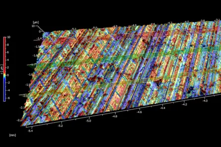
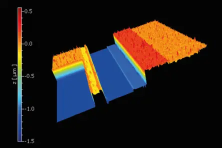
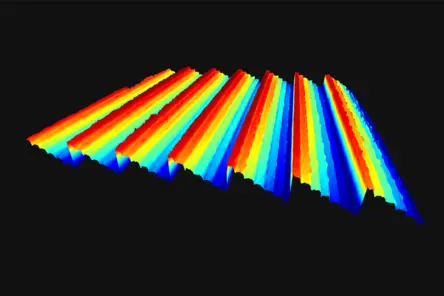
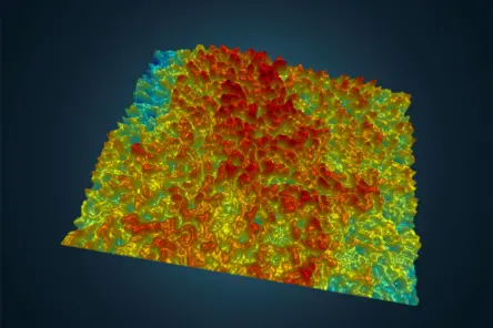
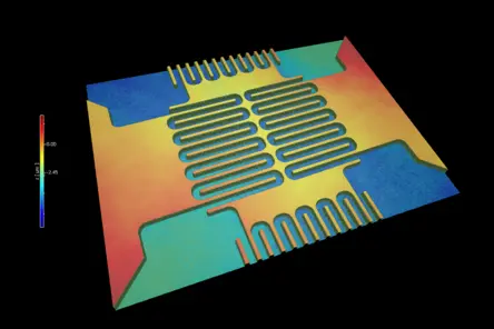
Here are some surface measurement examples—from roughness, tribology measurement to analyzing microstructures.

Profilometer Q&A and related articles for profilometers in regards to our optical profilers
We gathered some questions, which customers ask when comparing optical profilometers, selecting a fitting system, or planning their metrology workflow.
What is an optical profilometer?
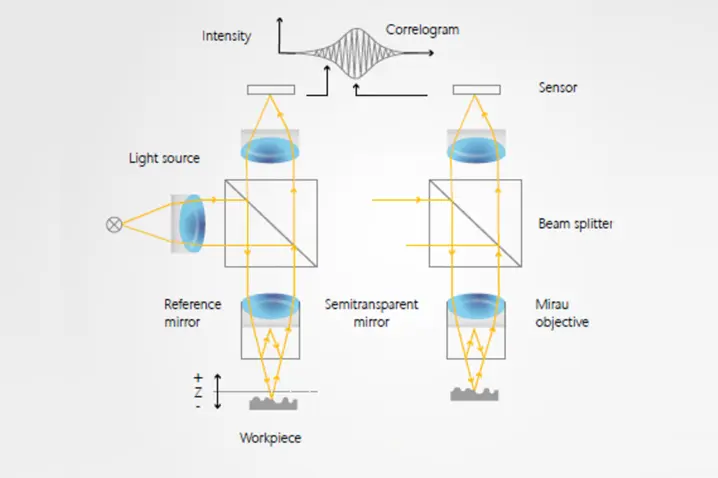
An optical profilometer is a non-contact measurement system used to capture 3D surface topography with high vertical resolution. Optical profilometers are commonly based on coherence scanning interferometry (CSI) and are used to measure surface roughness but also form, flatness, step height and microstructures across a wide range of materials.
Are companies shifting from their installed profiler to Polytec systems? And if so - why?
Yes — many companies transition from existing profilers to Polytec when their applications become more demanding. Their systems reach limits – for example with challenging materials (such as highly reflective surfaces), growing sample sizes and stitching quality, or the need for higher automation. Polytec systems excel in such areas - difficult to measure surfaces, large-area measurement and reliable, precise stitching.
The investment in a surface profiler is a significant decision - from a cost perspective but also the effort on your site (training, integration, ...). Thus, we recommend to thoroughly test and evaluate potential systems. We from Polytec offer feasibility studies, PolyMeasure and PolyRent for a future-proof investment decision.
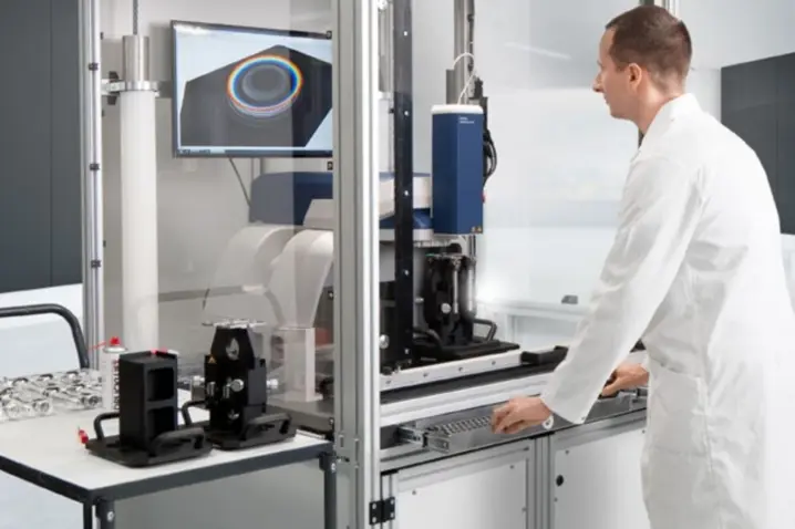
How can you help me in identifying the right system? What is the try-before-buy offer?
Surface profilers are a significant investment. It’s only natural to ask whether a system will support your short- and long-term needs and align with your metrology strategy.
With try-before-buy we want to support you in finding the best fitting profiler directly from the start. This lets you validate performance, workflows, and ROI before investing.
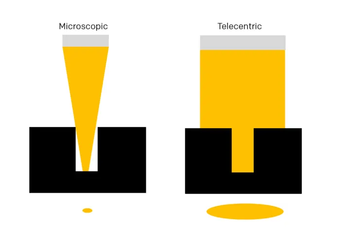
Micro vs macro profiler - When to use what?
Large area systems with a telecentric configuration allow you to simultaneously and quickly measure the topography of large surfaces in a single measurement. Optical profilers based on microscope systems, where the optical configuration including the reference arm is integrated into the lens, are more suitable if you require more lateral details on the whole area.
Microscopic systems (Micro.View)
- Small FoV
- Highest lateral resolution
- Best for microstructures and MEMS
- Trade-off: lower throughput on large samples
Macroscopic systems (Pro.Surf / Metro.Lab)
- Telecentric optics, large FoV
- Ideal for trays, flatness, parallelism
- Best for larger components
- Trade-off: lower lateral detail than microscopy
Rule of thumb:
- Need micro-scale detail? → Micro.View
- Need large-area form (flatness, parallelism,..) ? → Pro.Surf / Metro.Lab
Microscope or telecentric optics for profilometers?
Telecentric optics (Pro.Surf / Metro.Lab)
...keep magnification constant across height and offer a long, safe working distance. On Pro.Surf and Metro.Lab this helps measure near steep edges and down into bores while maintaining scale accuracy — ideal for flatness/parallelism on larger parts.
Focused, microscope optics (Micro.View)
....prioritize lateral resolution on small fields for rich details and sub-nm analysis. They excel at micro-features and surface finish but typically have shorter working distances, so access to deep holes/edges can be more constrained.
Why is stitching highly relevant for wider samples? What is "True Stitching"?
Because larger surfaces exceed the single-shot field of view — stitching merges tiles into one accurate dataset.
When the area to be measured exceeds the single-shot field of view (FoV), the system must acquire multiple single measurements and stitch them into one areal dataset. The metrology quality of such large-area measurements depends on the optics and sensing technology, the number of tiles and the stitching algorithms.
True Stitching delivers high-fidelity large-area measurements by minimizing stitching artifacts and preserving geometry.
An independent benchmarking at a leading German technical university compared six optical profilers from different manufacturers and the Polytec profilometer demonstrated the highest stitching and measurement quality. This is achieved by various features as:
- Large single-shot FoV → fewer tiles and seams, less cumulative error
- Sophisticated stitching algorithms → controlled overlap, robust registration, and metrology-safe blending that preserves steps and edges
- For Pro.Surf: Telecentric/CSI optics with correlogram evaluation → stable geometry and height fidelity across tiles
The result is high-fidelity, large-area topography with fewer artifacts and audit-ready residuals—what we call True Stitching.
Are TopMap profilers ready for production?
Due to the rugged design with very limited to no moving parts, SST (Smart Scanning Technology) and ECT (Environmental Compensation Technology), the Pro.Surf line and Micro.View+ are ready for in- and at-line metrology. Also Metro.Lab, as an easy to use bench solution, is an often used at-line quality control system.
Another advantage is the modular design of Pro.Surf and Micro.Surf. The sensor heads can be utilized as a single unit and by this easily integrated into your process.
So yes - Pro.Surf and Micro.View+ are ready for in-line and at-line integration thanks to rugged mechanics and stable sensing technology as fitting features.

What is the warranty for the Polytec optical profilometers?
Polytec stands behind the durability and performance of its surface metrology systems by offering a unique 4-year warranty, reflecting our confidence in the quality and longevity of our optical profilers.
White light interferometer
Introduction of the white light interferometry technology and the benefits for non-contact areal surface measurement.
Surface parameters
Learn more about roughness, flatness, step-height and layer thickness.

"Try before buy" offer
Measure, rent, decide - on your terms. Make a confident decision about which surface profiler fits into your metrology strategy and safeguard your capital investment.
Discuss your demands with our experts
Let’s start with a short discussion about your parts, tolerances, and workflow—and, if useful, we can add a feasibility study, PolyMeasure (contract measurements), or a PolyRent trial as optional next steps.